


Within the first few pages of IPC standard for printed circuit boards, there is a reference table 1-2 that is called “Default Requirements.” When reading the standard looking for some guidance, one may question “default” as part of a requirement. Often, when we receive circuit board production files there is not enough information from a manufacturing standpoint but certainly enough to quote.
There may be enough information to build the circuit boards as long as there is set manufacturing guidelines for processing to meet.
But is that enough? In this post, we will review some items you should be aware of.

Supply Your PCB Data with Documentation
Often, the missing information is the smaller details. Epec’s customer success managers are technically trained to review all items supplied to Epec for quoting purposes. During the review of provided documentation items such as print notes containing material requirements, specifications, surface treatments, copper weights, layer count, test analysis details, and other items are needed to calculate cost. It is possible to provide a quote without specific details needed for manufacturing of the PCB.
So, what information is missing that is needed?
Understanding PCB Material Tolerances
Regarding PCB laminate materials, providing specific Tg rating (transition of glass) is commonly listed as FR4, 170Tg, and 180Tg. Keeping material listed as basic Tg required and not noting by brand allows for manufacturing to use common material stock. Providing a stack-up with specific dielectrics when needed is a trigger for reviewing in more depth. Stating the overall printed circuit board thickness is critical to production selection of the appropriated materials to be used.
A tolerance less than 10% of the required finish can push the quote to engineering review and delay processing. For example, a 6-layer PCB could require 0.014” cores to be used and to meet 0.062” thickness. This is extremely doable however the remaining materials for build are left to assumption and will fall within +/-0.0062” of the total thickness. The finished parts will be 0.056” - 0.068” thick and can be a variation in between those. It is impossible the meet the exact overall and a tolerance is always needed.
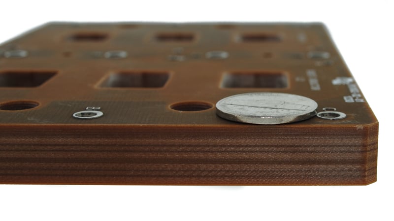
Example of an extremely thick PCB in comparison to a nickel.
For less than 10%, a change in the core may be required, as well as tighter process control and added cost. Selecting and measuring cores and materials is a time-consuming process that can be done at the prototype stage, during production volumes and is much more costly. Using a variation of the 10% should also be considered for example 0.062” +0.010”/-0.002” or +0.012”/0.000”.
Understanding PCB Drill Tolerances
PCB manufacturing tolerances are another item commonly missed when creating a fabrication document package. Every aspect of manufacturing a circuit board has a built-into manufacturing tolerance. Some of the time the tolerance asked for is not enough.
Hole sizes for one item are not as simple as one would think. So, holes come in all sizes? During the design phase, component directly relate to the PCB and call out a specific drill size to be used. For plated holes and non-plated holes, the drill chart is critical for manufacturing as a guide for production. List the hole size as a finished desired hole. For plated holes allow for +\-0.003” for the tolerance and for non-plate +\-0.002”.
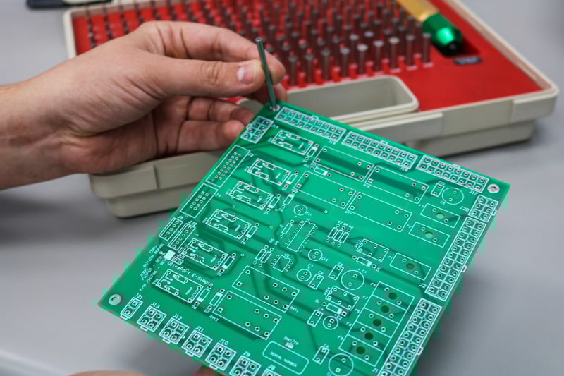
Printed circuit board being inspected for finished drill hole sizes.
Why is this?
Drills are purchased at specific sizes. Those sizes have a strict tolerance and are a machined part so naturally they measure up to the desired size, with a tolerance. For production, we increase the desired finished hole size by 0.005” - 0.006” to allow for processing. This is standard. A 0.040” desired hole finish will be drilled with an 0.046” diameter drill. Processing is not perfect, plating baths, time in/time out of tanks, additional plating, etching, more plating, finished plating all decrease the started hole size. Ultimately when completed, these holes are pin checked for accuracy and measure within the allowed tolerance of the size. Some of the time a desired hole of 0.040” will measure 0.040”, 0.041”, 0.038”, it can vary, thus the need for tolerance.
In some cases, a press fit hole, a tighter tolerance is required, +\-0.002” or smaller these should be noted on the drill chart for special handling, special drills, and process controls. The same goes for non-plated, +\-0.002” is needed for drill size compensation, there is no plating to be concerned with however not all drills are exact and a tolerance is needed. +\-0.002” or a total of 0.004” spread.
Larger holes plated or non-plated above the size of 0.200”, will commonly be routed, due to the routing process the following guidelines will apply to larger routed holes. A tolerance of +\-0.005” will apply.
Understanding PCB Routing Tolerances
Routing is also a process that needs a tolerance from slotting tools to routing cutouts or the PCB profile this process although accurate, a tolerance is needed. A typical tolerance of +\-0.005” is standard on the size or cut that is required. Small radius less than 0.040” require a special tool however will fall within the same +\-0.005” tolerance. Plated slots or non-plated slots will be calculated with a radius, considering the actual needed is critical to note on the documentation with a tolerance that considers the radius.
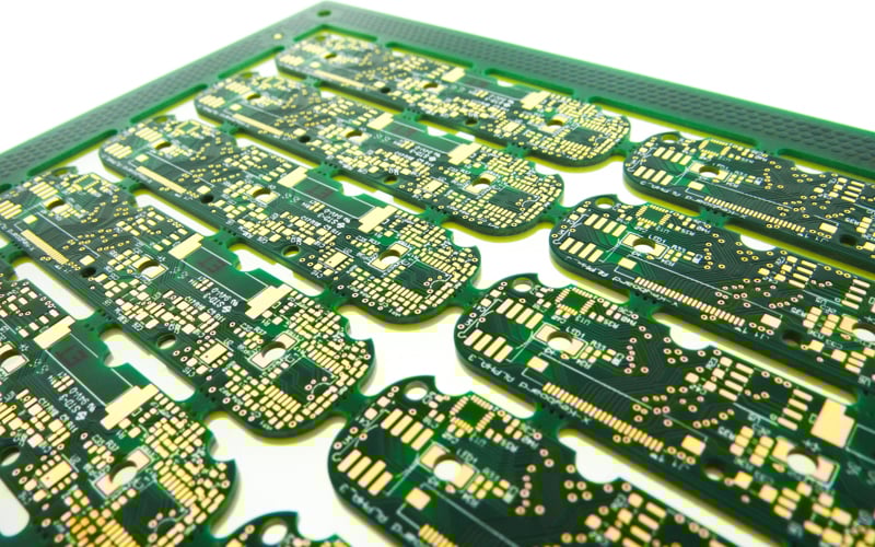
Example of PCBs in an array with rounded routing features.
Considering the process of routing slots, the router bit has an entry position X/Y and a lift or exit stop position at X/Y the distance between the two locations the router remains engaged with the material. The smaller diameter slots may need to be routed with a pecking drill that will have a plunge and exit, however, all space between the drill will exit and reenter the material leaving the walls of the slot somewhat imperfect.
When is it OK to Not be Specific?
As mentioned, the IPC has standards for printed circuit board and flex circuit qualification and performance specifications for manufacturing to use as a guide when processing. We still need your guidance on basics such as surface finish, PCB thickness, copper weights, mask and legend colors, holes sizes, and materials. For PCB manufacturing, the guides will always be referred to when specifics are not provided within the data package.
Summary
Tolerances are critical to our process to allow us to manufacture circuit boards in a standard process setting. A good data package will include tolerances and details eliminating defaults or delays in production.
When all the details add up, everyone benefits from quality product including assembly and final assembly. Ask an engineer at Epec for a free DFM, including tolerance advice, fabrication, and array layout.
Key Takeaways
- Complete documentation is essential: Supplying detailed PCB data, including stack-ups, Tg requirements, thickness, drill charts, and finish notes, ensures accurate quoting and smooth manufacturing without delays.
- Material thickness tolerances affect cost and manufacturability: A standard ±10% tolerance is common, but tighter requirements may force material changes, increase process control needs, and raise costs.
- Drill hole tolerances must be realistic: Plated holes should allow ±0.003” and non-plated ±0.002” due to plating variations, drill wear, and process factors, with special handling required for tighter tolerances.
- Routing tolerances are typically ±0.005”: This applies to profiles, slots, and cutouts, but very small radii or plated slots may require special tooling and should be clearly noted in the documentation.
- Relying only on IPC defaults can cause issues: While IPC provides general guidelines, customer-specified tolerances and details for critical features prevent delays, rework, or mismatches during PCB production.


