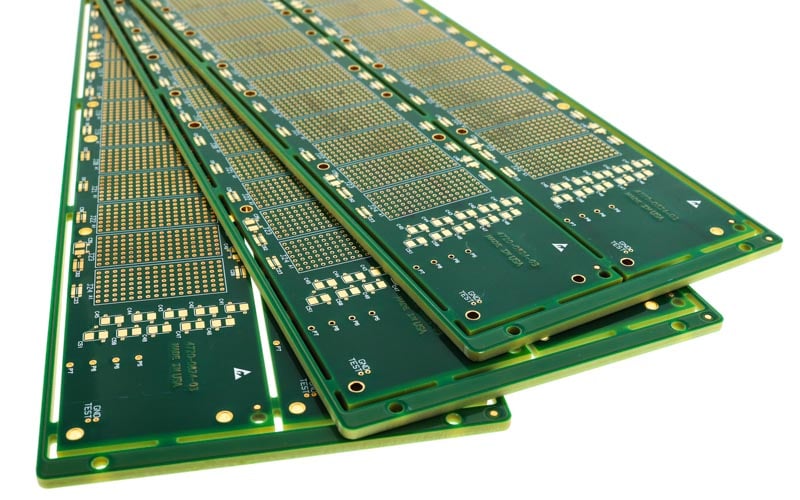
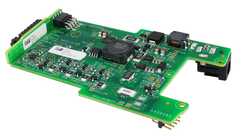
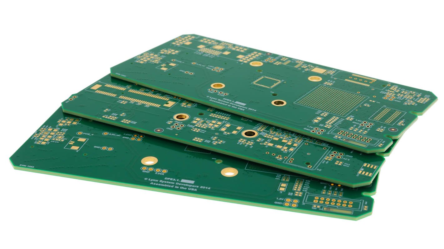
Many engineers and buyers assume that printed circuit board (PCB) manufacturers are only interested in large production volume orders. It is an easy conclusion to draw. High-volume manufacturing often dominates industry conversations, and many suppliers structure their operations around scale. But the reality is very different for companies like Epec, which specializes in high mix, low/medium volume-engineered products like PCBs.
Read MorePrinted circuit board assemblies used inside battery packs operate in a uniquely demanding environment. They are often enclosed, exposed to temperature swings, subjected to charge and discharge cycles, and expected to perform reliably for years without service.
Read MoreWhen a printed circuit board (PCB) overheats in the field, the root cause often traces back to one simple question that was never fully answered during layout: how much current is really flowing through each trace? Trace sizing and copper weight decisions may seem routine, but small assumptions at this stage can lead to voltage drop, excessive heat, and long-term reliability problems.
Read MorePrinted circuit board (PCB) field failures are among the costliest issues electronics companies face. A circuit board that performs perfectly in the initial testing process but fails in the field can be catastrophic. Performing design-for-manufacturability (DFM) on the PCB data before production manufacturing begins prevents oversights that could have been prevented early in the product lifecycle.
Read MoreEffective thermal management is a crucial aspect of multilayer printed circuit board fabrication. As circuit density and power requirements continue to increase, so does the potential for heat buildup within a board’s layers. Without proper control, excessive temperatures can cause delamination, warping, component failure, and signal instability.
Read MoreIt’s no secret that as printed circuit boards (PCBs) have evolved into higher technology levels, it has become more difficult to process the boards in a standard production setting. By standard, I mean panelized boards popped onto the line or conveyor and letting them run. Copper is the driving processing factor for a lot of production; the ounce weight drives the part and determines how long.
Read MoreI have spoken in the past about my long career in printed circuit board (PCB) manufacturing (1982) and how, at the beginning of my career, we still had home phones tied to the wall by cord. If we were lucky enough, the spiral stretch cord was very long.
Read MoreIn modern electronic systems, the need for high-speed data transmission has never been greater. With faster clock speeds, smaller geometries, and increasing complexity in printed circuit board (PCB) layouts, ensuring signal integrity has become a top priority for designers. Consulting your PCB manufacturer should be at the top of your list.
Read MorePrototyping is one of the most critical stages in the development of any electronic product. A well-designed printed circuit board (PCB) prototype can help you validate your concept, detect flaws early, and streamline the transition to production.
Read MoreWhen I first started thinking about printed circuit board (PCB) testing, my immediate reaction was boredom. Let’s be honest, it doesn’t have the hands-on excitement of building the circuit board itself. You're not designing the PCB; you're just running it through a tester, sorting it into a pass or fail bin, and moving on. I’ve done the job myself, so I know how repetitive it can feel.
Read More


