


Contrary to some customers’ perspectives, flex circuits are not indestructible. As with any part that contains a metal if it is bent or handled beyond its physical capabilities it will break. In this blog, we will cover the 3 main causes of fractured or cracked circuits in a flex design and how to prevent them from occurring. We’ll also review how to determine the minimum bend capabilities of a flexible circuit board design.

Minimum Bend Capabilities
A primary failure method involves exceeding the minimum bend radius capabilities of the materials that comprise a flex circuit. Specifically, the copper circuit layer(s). The minimum bend radius differs depending on the application.
The most common type of flex circuit is the static bend. A “one-time bend” in an application where a flex circuit is bent into position one time to fit into the assembly and then does not significantly move again unless the unit is being serviced. For the static bend, the common issue causing a trace fracture/crack is that the bend itself is too tight and exceeds the capabilities of the material. The minimum bend radius, and we'll define this a little bit later in this post, is critical for a static bend application, even though it's bent once. It is also common to encounter situations where the flex must be bent multiple times to perform or facilitate the assembly process. Bending the flex two or three times combined with an excessively tight bend radius is a primary root cause for fractured traces.
Another common flex circuit is a dynamic bend. This is used in applications where the flex circuit is bent and unbent many times as part of the function of the final assembly. A common example of a dynamic bend is a flex cable in an inkjet printer that cycles back and forth connecting the printer head to the main electronics. For the dynamic bend application, the common scenario is the copper work hardening after X number of cycles. Again, because the minimum bend radius for the application is being exceeded. It only needs to exceed the minimum bend by a small amount but when combined with many operational cycles, copper as metal, when taken beyond its point of ductility work hardens. Each cycle of work causes the copper to harden slightly and start to embrittle and after X number of cycles, the copper circuits will start to crack.
ENIG Surface Finished Pads/Traces
The second failure mechanism is bending a flex circuit immediately adjacent to an unsupported ENIG surface finished pad. ENIG is composed of two materials, an initial layer of nickel deposited on the exposed copper pads and a gold layer that encapsulates the nickel. Nickel is a relatively brittle metal and cannot withstand bending to any significant degree. Any surface mount or PTH feature, that has a trace connecting to it on an external layer, will have a small portion of the trace exposed leading from the edge of the pad to where the opening of the coverlay starts. This exposed trace section will also be encapsulated in ENIG. If ineffectively or unsupported by a stiffener and the flex is bent immediately adjacent to that pad, there is a high likelihood, that the ENIG encapsulating the trace segment will crack. This creates a significant mechanical stress concentrator on the underlying copper trace which results in the ENIG crack propagating through the copper trace.
A similar scenario as the above involves ZIF connector applications and occurs at the edge of the coverlay that exposes the ZIF contact fingers. If the flex circuit is mishandled during installation and inadvertently bent at this location, the same situation occurs when the ENIG surface finish on the ZIF contacts cracks and creates a crack in the copper contact fingers.
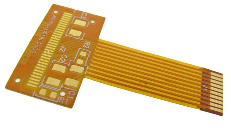
Flex PCB with FR4 stiffener supported component area and ZIF contacts.
Mechanical Stress Concentrators
The last failure mechanism is due to mechanical stress concentrators that exist within an inadequate design. These stress concentrators may lead to a flex circuit kinking sharply, with a tighter bend radius that exceeds the material properties, than was intended instead of allowing the flex to take a smooth arc with the largest possible bend radius. Mechanical stress concentrators can inadvertently be created by the layout of the circuitry in the bent areas of a flex design, the shape of the flex circuit outline, the location of stiffeners, via or PTH holes in the flex area, or the configuration of the coverlay layers.
The second scenario can occur in a rigid-flex construction where the flex is bent tightly adjacent to the transition from the rigid area(s) to the flex area(s). This transition creates a very sharp mechanical stress concentrator, which can cause the flex to kink and bend sharply rather than take a smooth radius and stay within its minimum bend capabilities.
Preventing Trace Fractures
Preventing fractured or cracked traces is dependent upon the flex design meeting the requirements of the project. During the manufacturing process, the properties of the materials cannot be altered.
Min. Bend Capability: The bend requirements of the application must be defined and included in the flex circuit design process to ensure that the material stack-up will meet bend requirements. Assembly considerations need to be included, i.e.: multiple bends required as part of the assembly process. Educating assembly technicians as to the limitations of the flex circuits is an important element to ensure that the parts are not inadvertently mishandled during the assembly process(s).
ENIG Surface Finish: As recommended by IPC 2223 flex circuit design standard, all component areas should be supported by a rigidizing stiffener that prevents the flex circuit from being bent in a soldered component area. This eliminates the opportunity for ENIG-related cracked circuits as well as potential solder joint reliability issues. Rigidizing stiffeners are typically FR4 materials ranging from 0.010” to 0.059” in thickness. Thin stainless-steel stiffeners can also be used if there is limited spacing available.
ENIG-related fractures at ZIF contact fingers can be addressed by educating the assembly technicians to ensure that the ZIF connector latching mechanisms are fully open prior to inserting the flex circuit. As the name implies it requires zero insertion force to fully engage a flex circuit into a ZIF connector. Once resistance is encountered the flex is fully seated, the ZIF latch can be closed to lock in the flex circuit. A closed or partially open ZIF will require excessive force to engage the flex which may result in the part kinking and creating cracks in the contacts.
Mechanical Stress Concentrators: For designs with a change in direction in a flexed area, it’s necessary to use rounded/radiused corners, with as relaxed a radius as the design allows, for both the circuits and the part outline. Ninety-degree corners are strongly not recommended and radiused corners are preferred over 45-degree corners.
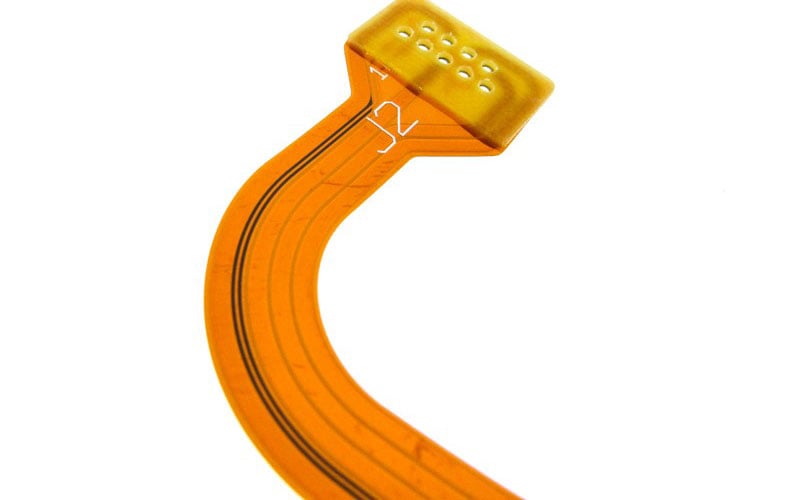
2-layer flex circuit with curved traces in bend area.
Rigid-flex designs, with tight bend requirements close to the rigid to flex transition areas, should utilize a flexible epoxy bead at the transition. This will ensure the flex takes a smooth radius when bent and does not kink at the transition.
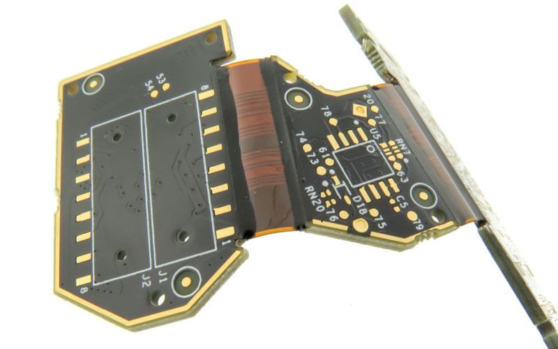
4-layer rigid-flex circuit board with epoxy strain reliefs at flex transitions.
It is not recommended for coverlays and stiffeners to start/stop at the same location in the design. If allowed the significant change in the thickness of flex creates a very strong mechanical stress concentrator. Stiffener shapes can also use pointed or rounded edges, as opposed to a straight edge, to help mitigate a stress concentrator. Via and/or PTH holes should be avoided in the flex area whenever possible and located in areas supported by stiffeners. If they are required, for example, to create an EMI faraday cage, the minimum bend capability of the design will be reduced.
IPC 2223 Minimum Bend Radius Guidelines
The minimum bend radius of a flex circuit is a function of the thickness of the flex circuit and the materials used. IPC 2223 Design Standard includes material property-based calculations for both static and dynamic bend applications. These calculations are fairly involved, and most applications don't require effort. The most common method in the industry is to use the general rules of thumb, which define min bend radiuses as follows:
For a static bend application, a 1-2-layer design minimum bend = 10X the flex thickness, 3 layers = 15 – 20X, 4 layers = 25 – 30X etc. For a dynamic bend application, the layer count is limited to 1-2 layers and the minimum bend radius is 100X the flex thickness.
Summary
The common denominator with all root causes of flexible circuit trace fractures is that of the design and the materials used. The individual root causes are also not always independent of each other and can accumulate to create a potential reliability issue. Please feel free to contact Epec to discuss your specific needs and to have your design requirements reviewed to ensure the reliability of your design
Key Takeaways
- Minimum Bend Radius is Critical: Exceeding the minimum bend radius, especially in static or dynamic applications, is one of the primary causes of cracked or fractured traces in flexible PCBs.
- ENIG Can Cause Stress Fractures: Unsupported ENIG-plated pads or traces near bend points are prone to cracking due to nickel’s brittleness. Supporting these areas with stiffeners is essential to avoid failure.
- Avoid Mechanical Stress Concentrators: Poor layout choices like sharp corners, abrupt stiffener transitions, and poorly placed vias can create high-stress zones that increase fracture risk. Use radiused corners and smooth transitions instead.
- ZIF Connector Mishandling Can Damage Contacts: Improper insertion into ZIF connectors, especially without fully opening the latch, can bend the flex and cause cracking in ENIG-plated contact fingers.
- Design for Assembly and Reliability: Meeting bend requirements, using proper stiffener support, and educating assembly teams on flex limitations are all vital steps to prevent damage and ensure long-term circuit reliability.


