


Rigid-flex PCBs are engineered to eliminate the very failure points introduced by traditional cable and connector assemblies, but they’re not immune to failure themselves. While rigid-flex technology reduces interconnects and improves signal integrity, it also introduces unique design and handling challenges. When not properly accounted for, these challenges can result in costly production issues, reduced reliability, or premature field failure.
For engineers unfamiliar with rigid-flex applications, identifying the root cause of a failure can be incredibly difficult. But with experience and sound design-for-manufacturing (DFM) practices, most rigid-flex failures are predictable, preventable, and avoidable with the right process.
In this blog, we break down the most common failure modes in rigid-flex PCB assemblies into two major categories: handling/bending-related errors and design-based errors. Understanding both is key to building a reliable, manufacturable product.

Handling and Bending Failures
These failures typically occur after the PCB is fabricated during assembly, testing, or even field installation. Most handling-related issues trace back to mismanagement of the flex zones, which can sometimes be more susceptible to handling errors than a rigid board.
Bend Radius Violations
One of the most frequent causes of flex circuit failure in rigid-flex circuit boards is ignoring proper bend radius guidelines. When a circuit is bent too tightly or repeatedly beyond its rated tolerance, the copper traces within the flex layer may work-harden and eventually crack, leading to intermittent opens or full circuit failure.
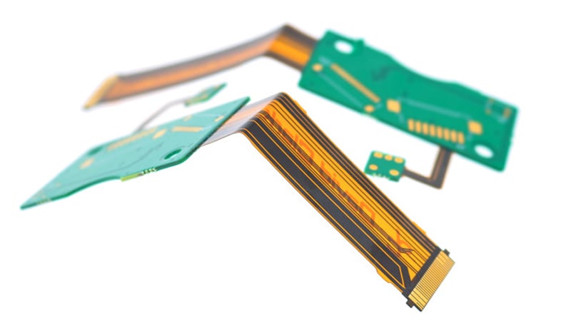
An example of a bend in a rigid-flex PCB where it is starting to deform and permanently crease.
In the worst cases, a tight bend results in a permanent crease, which cannot be reversed and typically compromises both mechanical and electrical performance. Designers must adhere to IPC-2223 bend radius guidelines, which vary based on material stack-up, number of layers, and whether the bend is dynamic or static.
Poor Bend Placement
Even when radius specs are followed, improper bend location can create mechanical stress near rigid interfaces. If the bend occurs too close to the rigid edge, prepreg or laminate material can protrude, potentially slicing or pinching the adjacent flex material. This is especially dangerous if untrimmed glass fibers or sharp edges are present at the transition.
Components on Flexible Sections
Another common misstep is placing components on flexible areas, particularly in zones that are expected to bend. This leads to two major risks:
- Cracked solder joints due to repeated flexing.
- Pad delamination or tear-out, especially with fine-pitch or BGA components.
The remedy is straightforward: relocating components to rigid sections or reinforcing the component zone using a stiffener. The stiffener provides mechanical support and helps isolate components from flex-induced stress.
Pre-Bake Oversight
Moisture trapped within the PCB materials can expand during solder reflow, causing delamination, bubbling, or popcorning. This is why pre-baking boards prior to assembly is essential, especially for designs that include polyimide layers, adhesives, and complex lamination. Skipping this step is a leading cause of handling-related field failures.
Design-Based Failures
Some failures are baked into the design from the beginning, literally. Even with flawless handling, an oversight during the design layout or stack-up creation phase can introduce vulnerabilities that emerge during thermal cycling, reflow, or mechanical operation.
Vias Too Close to Rigid-Flex Interfaces
Placing vias near rigid-flex transitions is a common error, especially when routing tight pin-pitch devices. This violates IPC-2223 design rules, as differing coefficients of thermal expansion (CTEs) between the rigid and flex materials can introduce stress at the via barrel. This may manifest as intermittent opens, via cracks, or even complete delamination during reflow.
Designers must observe minimum clearance rules for via-to-interface placement and consider terminating via structures in fully rigid areas when possible.
Sharp Trace Angles in Flex Regions
In the flexible layers, routing matters more than many realize. Traces with sharp corners or abrupt turns can act as stress concentrators, especially in areas subject to repeated bending. This creates a failure point in the copper that can propagate over time, leading to circuit fracture.
Use gradual, curved routing with generous arc radii to minimize mechanical strain and evenly distribute stress during flexing.
Stiffener-Related Failures
Stiffeners are often added as an afterthought to reinforce flexible areas, but poorly planned stiffener placement can create new failure points. If stiffeners are too close to vias or lack adequate overlap with coverlays, mechanical stress can concentrate at the interface, causing via cracking or delamination under load.
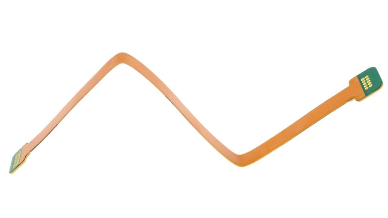
A flexible PCB with stiffeners that are only placed in necessary locations far away from bend areas.
To avoid this, ensure stiffener overlap is sufficient and placed strategically away from critical interconnects. Also, coordinate stiffener design with the manufacturer to verify material compatibility and thermal expansion alignment.
Imbalanced Stack-ups and Warpage
A common but often overlooked design flaw is using an unbalanced stack-up, especially in asymmetric rigid-flex constructions. This can lead to warping, twisting, or bowing in the rigid regions, making the board difficult to assemble or incompatible with enclosures.
Always aim for symmetrical stack-ups where possible. An unbalanced build doesn’t just cause handling issues; it can also stress solder joints and introduce long-term reliability risks.
Summary
While rigid-flex PCBs reduce failure-prone interconnects, they aren’t immune to failure themselves. The key to reliability lies in good design practices, proper DFM reviews, and rigorous handling procedures.
Some failures, like delamination or via cracking, are obvious. Others, such as field failures due to intermittent signal loss, can take weeks or months to identify. But nearly all rigid-flex failures fall into predictable categories and can be prevented with the right expertise.
At Epec, we help customers catch these failure modes before they happen. From bend analysis and stiffener placement to DFM for via clearances and impedance tuning, our engineers are here to ensure your rigid-flex design is robust, reliable, and ready for production.
Key Takeaways
- Bend radius violations and poor bend placement are leading causes of mechanical failure in flex circuits.
- Vias near rigid-flex interfaces are highly vulnerable and should follow IPC-2223 spacing guidelines.
- Component placement in flex zones can cause cracked solder joints and pad delamination; use stiffeners or relocate to rigid areas.
- Stack-up symmetry and stiffener strategy are critical to prevent warpage and mechanical stress.
- A proactive DFM review with an experienced manufacturer is your best defense against design-induced failure.


