


Many of today’s rigid-flex circuit designs utilize the same high-density components found in rigid PCB designs. This requires the use of blind and or buried vias to allow the signal lines to be routed out from within the high-density components or the high-density areas of the design. The most common component that we see driving this today is the 0.4mm pitch BGA package.
Blind vias allow the signals to be dropped down to the next layer from within the BGA SMT pad and then routed out from there. In high pin count devices, additional blind and or buried vias may be required. Differences exist in how blind and buried vias can be implemented in a rigid–flex design due to the materials and manufacturing processes required.
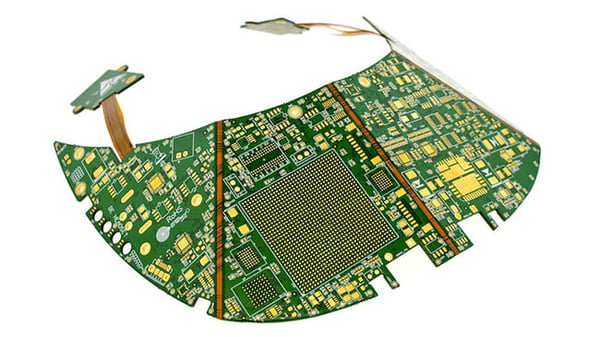 Complex Rigid-Flex Circuit Board
Material Requirements
A key difference from rigid PCBs is the type of pre-preg used to both bond the rigid layers together and the rigid layers to the flex layers. Specifically, a “No-Flow” pre-preg is required. The pre-preg does flow but the extent of its flow characteristics is limited. This pre-preg is the same material as full flow pre-preg used in rigid PCBs but is cured to a higher state by the material supplier. No-Flow pre-preg prevents the material from flowing or extruding out onto the surface of the exposed flexible areas. If this occurred, the parts would fail as soon as they were bent into position. A byproduct of the limited flow characteristics is that a thicker amount of No-Flow pre-preg is needed to ensure that the circuitry is fully encapsulated, and a proper lamination bond achieved. This increased pre-preg thickness may impact the design by increasing the blind via aspect ratio beyond the 1:1 limit.

An added element is the copper thickness specified for the internal layers. Thicker copper requires thicker pre-preg layers to ensure full encapsulation which may then limit the application of blind vias due to the aspect ratio limits.
Number of Lamination Cycles
A common requirement in buried via designs is the need for multiple or sequential lamination cycles. This allows the internal buried vias to be drilled and plated and then additional layers laminated to the part to complete the entire layer structure.
Rigid–flex designs are limited in the number of sequential lamination cycles that can be performed due to both the materials used and the manufacturing methods. The internal polyimide flex layers have a much greater dimensional tolerance than rigid materials. The rigid and pre-preg layers, in most designs, must have areas that will be flexible sections removed prior to lamination. Removing these sections of material destabilizes the rigid and pre-preg layers adding further dimensional tolerances. These two items combined increase the extent to which the dimensions of the part will change when subjected to the heat and pressure of the lamination processes. This can reach the point where layer to layer alignment and overall part dimension tolerances can no longer be achieved. For most designs, the practical limit is 2 lamination cycles.
The number of lamination cycles in a rigid–flex design will impact the number and configuration of blind & buried via that can be implemented.
Blind & Buried Via Material Stack-Ups
While there are potential constraints with blind and buried vias that need to be factored into a rigid–flex design, there are a wide variety of configurations that can be applied to resolve high density routing requirments.
The 1st example is a 6-layer construction with 2 flex layers. This utilizes 2 blind vias from the external layers down to the next internal layers and 1 internal buried vias between the flex core layer pair. This construction does not require any additional or sequential lamination processes.
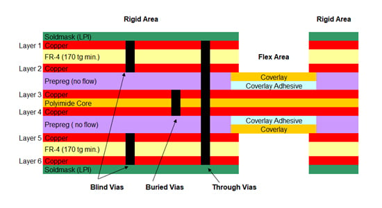 6-Layer Rigid PCB Construction with Two Flex Layers
The 2nd example is a more complex 8-layer design with 2 flex layers. A sequential lamination cycle is required. Layers 2-7 are laminated together and blind vias from Layers 2 to 3 and from layers 7 to 6 as well as the buried via from layers 2 to 7 are drilled and plated. Layers 1 & 2 are then laminated using a foil outer construction method and blind vias from layers 1-2 and from layers 8-7 and the through vias from layers 1-8 are drilled and plated.
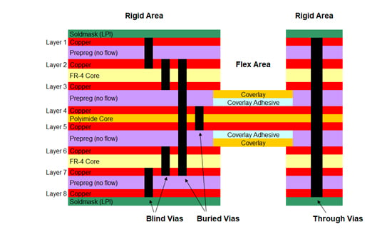 More Complex 8-Layer Rigid PCB Design with Two Flex Layers
A common item with both above configurations is that the finished thickness may be limited by the blind via requirement to maintain a max 1:1 aspect ratio. If a specific thicker rigid area dimension is needed it may be achieved by adding additional layers of FR4 and pre-preg.
Controlled impedance requirements may also impact the design due to the dielectric spacing between layers required to achieve the specific impedance values.
Via in Pad & Via Fill
Many designs that utilize blind and buried vias also require the blind and/or through vias to be located within the SMT pads on the external layers. This then requires the vias to be filled and capped with copper to ensure a flat co-planer SMT pad and to prevent solder from being drawn into an open via which could potentially starve the solder joint of solder. This process is the same as the rigid PCB process and can be applied to all rigid-flex designs.

Summary
The use of blind and buried vias in rigid-flex designs is a very common requirement today but has a different set of design rules due to the materials and manufacturing process involved.
We recommend discussing with an engineering group early in the design phase to reach specific requirements. This will prevent the creation of a design that is either cost prohibitive, potentially not manufacturable, or ultimately will not meet all your design requirements.
Key Takeaways
- Material limitations affect via design in rigid-flex circuits: Unlike rigid PCBs, rigid-flex requires No-Flow pre-preg to prevent resin squeeze-out into flex areas. This thicker pre-preg can increase blind via aspect ratios beyond the recommended 1:1.
- Sequential lamination cycles are more limited in rigid-flex: Due to dimensional instability of polyimide flex layers and pre-preg cutouts, most designs are limited to two lamination cycles, which constrain blind and buried via configurations.
- Design stack-ups must balance vias and flexibility: Common examples include 6-layer constructions with simple blind and buried vias (no extra lamination) and more complex 8-layer builds requiring sequential lamination and multiple via types.
- Finished thickness and impedance requirements are tied to via structures: Blind via aspect ratios, added FR4 layers, and dielectric spacing for impedance control must all be factored into rigid-flex layouts.
- Via in pad and via fill follow the same process as rigid boards: When vias are placed in SMT pads, they must be filled and copper capped to ensure a flat solderable surface and prevent solder wicking, ensuring assembly reliability.


