A common misconception for ordering PCBs online is that it can only be low technology/low quantities for prototypes, but that is not the case. At InstantPCBQuote™, we have the capabilities for you to order circuit boards up to 16-layer with high-temp materials, blind and buried vias, and with controlled impedance.
As more and more PCB manufacturers move to an online model, it is best to know where and how your circuit boards will be manufactured. A PCB shop with limited equipment may not be able to produce some higher technology boards in-house. Risk is also a factor. Are you going to order a 16-layer PCB online directly from an Asian manufacturer’s website? Probably not, but it happens, and there are those who are fine with ordering 3 PCBs for $33.00. It’s cheap, but not always the best solution when quality and reliability issues come into play.
This also raises some questions regarding best practices for ordering high-tech PCBs online.
In this blog post, we will walk through the items needed for moving your printed circuit board purchased online to your dock smoothly, including what to do and what not to do.

The Online PCB Order
My first piece of advice and probably the most important one is: do not wait until the last minute. Although many of our customers use InstantPCBQuote™, our online PCB ordering system. By now, everyone has heard of all the horror stories when trying to manage transportation, but Epec manages the shipment so delays are not likely to happen, or, if they do, we will rectify it quickly. Ordering printed circuit boards online and shipping them small packages given all the issues with freight both domestically and internationally can be a challenge. Time is of the essence and waiting could cause delays.
Don’t be afraid to use online ordering and quoting for high-technology PCBs as with InstantPCBQuote™ every job goes through a full DFM review, so if there are issues, we will catch them and work with you before we start production. We will discuss later in this blog post some of the items that cause issues as the layer count increases, but a 12-layer PCB with no blind/buried vias are regularly ordered and delivered by Epec from our online PCB tool.
Circuit Board Data Set, Panel Drawings, and Details
What is needed to make the transition from your online PCB order though delivery goes smoothly? We know from years of experience that there is a huge difference in data sets. Our customers are OEMS, CMs, and small engineering firms, and from each customer there can be many different design packages. A great data set is key to a smooth transition from purchase to production to receiving a quality product without delays delivered to you on-time.
We see hundreds of data sets monthly in the quote stage, ordering, and in engineering. We offer a free DFM service to aide our customers with manufacturability and to make sure data sets are complete and the data is accurate. But what is needed? All individual copper layers circuitry and ground planes should be drawn in a positive or negative format. The preferred data format is RS274X. The RS274X format is user-friendly and easily imported into most CAD systems without any manual input of apertures to complete the file set.
PCB Outline
For ease of manufacturing, always supply a 1-to-1 outline of the printed circuit board profile. Manufacturing will use the board outline for data set up, drilling, and routing programs as well as score details if needed.
Hole Sizes
With a drill program in Excellon format, be sure to include tool sizes that are the desired finished hole size. Production will size the actual drill to accommodate for the finished desired hole. Include a drill chart when possible that states the hole size desired, if the hole is plated through or non-plated, the quantity of each hole, and the specified tolerance allowed. Keep in mind standard manufacturing tolerances for plated holes are +\-0.003”; non-plated holes are +\-0.002”.
Soldermask
Also, include soldermask for both sides, specify the color desired, and keep in mind that green is the most widely used color in the industry. Although many colors are produced, not all manufacturing services will provide all flavors. Clearing and sizing soldermask files will be completed at the manufacturing facility; when special sizing is required this should be noted.
Keep in mind, processing colors other than green can lead to issues on copper-to-copper spacing less than 0.009”. The pigment changes and chemistries used on final finish can negatively impact the solder masking process, which leads to another need for production is the required surface coating.
Silkscreen
For silkscreen legends for one or both sides, specify the color only. For printable, legible font use a minimum character width of 0.005” and a height minimum of 0.035”. Smaller than these sizes may not reproduce in standard processing. Resizing is not a capability within CAD systems; we are able to clip and move the text only.
Fabrication Drawing
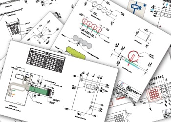
The fabrication drawing should contain information such as a dimensioned board outline and defined tolerances. The holes should be charted and noted as finished size with a tolerance and if they are plated through or non-plated. A good set of fabrication notes contains the details about the PCB. Not all supplied PCBs for manufacturing come with complete information, and that is OK. There are details that we do need to know: the copper weight of the internal layers and the final copper weight of the external layers. Listing the copper details as finished is a good way to describe the weight.
Noting the RoHS, specification, and class are also beneficial for quoting a PCB accurately and ensuring a smooth transition to production. Class II or III are typical for printed circuit board manufacturing. Class II is standard processing whereas Class III requires specialty processing, added cost, and final documentation. Not all facilities can produce Class III PCBs, so know your supplier.
Determining if your PCB is Considered a High-Tech Circuit Board
Defining high-technology PCBs can be difficult. There are many attributes that can push a standard printed circuit board into the higher-tech field, but how do you know? Besides the obvious items like blind or buried vias, via-in-pad process, layer counts about 8 to 16, small line widths <0.005”, hole size <0.008”, heavy copper greater than 4oz, thick PCBs over 0.125”, the list is long.
A good example of a simple 4-layer PCB that can be considered higher technology is if the design has tighter trace and space widths than the desired copper weight can support. For example, 0.005” trace with 0.005” space will process easily on 1/2oz copper weight. Increase the copper weight to 1oz for the same trace, and spacing and processing is no longer standard. The copper weight quickly doubles in thickness, making the smaller trace and space widths much more difficult to reproduce. Allowing for more space and modification for processing in tighter trace and space is a must on higher copper weighted materials.
Six to 16-layer PCBs are considered to be high-layer count and higher technology printed circuit boards. The higher the layer count, the more complex the process of manufacturing can be. Many higher layer counts will contain blind and/or buried vias. Multiple sets of these types of holes add to the complexity of the order. Each set of vias must be processed within its layer stack individually. The sets of vias from the entry to the exit layer will depend on the multiple passes; the part will go through the drilling, plating, and lamination processing. Blind and buried vias can add many hours of production time to the order, increasing the risk of scrap and adding cycle time to shipments. Lamination cycles are time-consuming as well as costly.
Another type of hole is a castellated hole. This hole is drilled on the board’s edge, half on, half off the PCBs edge. The hole will need to be primarily drilled into the PCB on the X, Y coordinate of the routed edge. The holes require primary drilling, plating, and special processing for routing so as not to lift or remove the plating barrel from the hole edges. The castellation is critical to end process assembly of parts. It is a difficult process; some curling, lifting, or burring cannot be helped, however, it can be kept to a minimum with special handling.
PCB overall thickness and specialized stack-up can also add to processing time. Specified dielectrics limit processing management of materials. The dielectric required to be met, and the common stock can also lead to a challenge in delivery if no material is on hand. Not all material thicknesses and copper weights are always in stock. Some come with a minimum to buy at a high cost. Online ordering is typical to lower quantity purchasing leaving specified dielectrics a problem to purchase materials from suppliers in lower volumes.
Soldermask is the coating applied to printed circuit boards to protect the copper surface, prevent oxidation, and shorting during the assembly process. The mask covering applied will allow for ease of assembly. Mask typically needs a 0.004” < spacing to adhere to the laminate surface and 0.003” < spacing to be relieved from copper surfaces a total of 0.009” from copper to copper is optimal. Less than 0.009” is more difficult to process; 0.008 is the bottom typically needed.
The one way to address all the previously mentioned issues is to have a conversation with your online PCB manufacturing partner about what you consistently put into your PCB designs. If we know that all of your designs will have a set of blind vias from another layer to an inner layer, we can change our program just for your username to add this cost into the program so that you can use the tool and not worry about the program or pricing being incorrect.
At InstantPCBQuote™ we have a significant number of customers where we have customized pricing programs that take into account their unique attributes so that they can use the tool 24/7 as it was meant.
Summary
Not all manufacturing resources should be considered capable to build all types of printed circuit boards, leaving some concerns when buying PCBs online. Although PCBs are built-to-print and unique, the processing of the part is the same in many of the steps. What makes the part tricky to build are the attributes, and not all manufacturing resources have the latest greatest equipment or skill to build all types. Using a trusted PCB supplier with skilled professionals and a strong capable supply chain is your best chance of online printed circuit board ordering success.
Key Takeaways
- Order Early to Avoid Delays: Time is the most critical factor when ordering PCBs online. Even with systems like InstantPCBQuote™, shipping and production logistics can still be affected by global transportation challenges.
- Provide a Complete and Accurate Data Set: Submitting detailed fabrication drawings, drill files, outlines, solder mask details, and copper weights ensures a smooth transition from quote to production without costly or time-consuming revisions.
- Know What Qualifies as High-Tech: High-technology PCBs often include blind or buried vias, high layer counts, tight trace and space tolerances, heavy copper weights, or special dielectric requirements, all of which increase complexity and processing time.
- Communicate with Your Supplier: For specialized designs, discuss your recurring design attributes with your online PCB supplier so they can adjust programs, pricing, and manufacturing processes specifically for your needs.
- Choose a Trusted Manufacturer: Partnering with an experienced PCB supplier that offers full DFM review, advanced capabilities, and a reliable supply chain minimizes risks and ensures consistent quality for high-tech online PCB orders.


