


At the conclusion of our webinar, Using Rigid-Flex PCBs to Improve Design Reliability, we had several questions submitted to our presenter, Product Manager of Flex & Rigid-Flex Circuits, Paul Tome. We compiled these into a readable format on our blog.
Q&A From Our Live Rigid-Flex Webinar
Quick Links:
- What general speeds (Gbps) are rigid-flex PWBs capable of supporting?
- What is the method of application of the EMI shielding films?
- We can only find 2223B available on the IPC website. How do we get 2223C?
- During the design of a flex/rigid PCB, are there ways to create a stiffer area where components would be placed (as part of the flex, not an added backer)?
- In a dynamic flex application where we are flexing rigid-flex combination PCB assemblies, what is the best way to specify construction, so we reduce failures at the rigid-flex interface?
- What are your HDI design rule requirements?
- Is coverlay needed if using a flexible shield material?
- On slide 17, what happens to the impedance of the controlled impedance when a flex is bent and then stray capacitance between the same trace occur? Do you have to always shield both sides in the flex section? What is the typical ER?
- What is the famous minimum spacing you are talking about in IPC2223C?
- Can the rigid-flex PCB handle 5KV input?
- Do flex only solutions provide the same reliability benefits as rigid-flex?
- What challenges do high-density BGAs create for class 3 rigid-flex?
- Can rigid-flex accommodate higher current carrying requirements?
- One question is regarding flex layer counts and their impact on reliability.
Watch the Recording Below:

Question: What general speeds (Gbps) are rigid-flex PWBs capable of supporting?
Answer: Rigid-flex are capable of supporting speeds similar to rigid PCBs. We have manufactured many designs for high-speed applications, but our customers do not typically divulge the operating speeds.
Question: What is the method of application of the EMI shielding films?
Answer: Shielding films are laminated under heat and pressure on to the surface of the coverlay(s). Selective openings in the coverlay(s) expose the ground net, and the conductive adhesive of the shielding film results in the shield becoming electrically connected to ground.
Question: We can only find 2223B available on the IPC website. How do we get 2223C?
Answer: IPC 2223 is now at Rev. D and is available at the IPC website: https://shop.ipc.org/IPC-2223D-English-P.
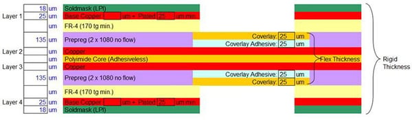
Question: During the design of a flex/rigid PCB, are there ways to create a stiffer area where components would be placed (as part of the flex, not an added backer)?
Answer: Integrated stiffeners or “rigidized areas” are created as a rigid-flex construction (see following material stack up example):
Question: In a dynamic flex application where we are flexing rigid-flex combination PCB assemblies, what is the best way to specify construction, so we reduce failures at the rigid-flex interface?
Answer: We see failures that look like the flex polyimide is pulled out of the rigid section. The common solution to prevent flex damage at the flex-to-rigid transition is to apply a bead of flexible epoxy. This ensures that the flex is strain relieved and that sharp bend is prevented. This is defined as a drawing note in the fabrication drawing.
Question: What are your HDI design rule requirements?
Answer: We have a wide variety of HDI capabilities of rigid-flex designs. To cover all of them would be a challenge in an email. We suggest that if you have a design in process that we set up a conference call to discuss your requirements in more detail.
Question: Is coverlay needed if using a flexible shield material?
Answer: Yes, coverlay is required when using shielding films. The coverlay insolates the circuit layer with selective openings exposing only the ground circuit. The adhesive layer of the shield film is electrically conductive and electrically connects the shield layer to the ground circuit during lamination.
Question: On slide 17, what happens to the impedance of the controlled impedance when a flex is bent and then stray capacitance between the same trace occur? Do you have to always shield both sides in the flex section? What is the typical ER?
Answer: Controlled impedance stays very consistent when a flex circuit is bent. There is no measurable change. Controlled impedance lines are shielded on both sides by means of using a stripline configuration with the signal lines sandwiched between two reference planes.
Question: What is the famous minimum spacing you are talking about in IPC2223C?
Answer: The minimum spacing discussed in our webinar is the distance from the edge of a plated hole or via to the transition from a rigid area to a flex area. IPC 2223 Sec. 5.5.2.3 & Figure 5-6 call out for 0.125” min. We are capable of achieving the intent of IPC with min. distance of 0.040” to 0.050” depending upon the design.
Question: Can the rigid-flex PCB handle 5KV input?
Answer: Yes, a rigid-flex can support 5KV. The flex layers have a dielectric withstanding of 5KV per 0.001” thickness. The same design rules for rigid PCBs need to be applied to the rigid areas of the rigid-flex, material thickness, line spacing, etc., need to be applied.
Question: Do flex only solutions provide the same reliability benefits as rigid-flex?
Answer: If the design has the components mounted directly to the flex, where the component areas are supported by stiffeners, then the answer is a definite yes. If the design is only a direct replacement for the wired portion of the design, then it's a yes, but to a lesser degree. The primary reason is it doesn't eliminate the points of interconnect, which is the primary benefit of rigid-flex. It still brings the benefits of reducing the weight, better bend capabilities, the durability in harsh environments, and so forth.
Question: What challenges do high-density BGAs create for class 3 rigid-flex?
Answer: This is actually a great question because we're working on many designs that fall right into this area. The solution that we've seen from the majority of customers is they will waive not all of class 3, but only the annular ring requirement in that specific BGA area, and it's just a function of the features getting so small.
Question: Can rigid-flex accommodate higher current carrying requirements?
Answer: As in most cases, the answer is a qualified yes. It's going to obviously depend upon the extent of the current and the available space within the design to use a preferred solution of increasing the width of the traces rather than increasing the thickness of the copper used for the traces. The issue with thicker copper relates back to the mechanical bend requirements in most flex designs. Copper is the is the stiffest component and has been by far the biggest impact on bend capabilities and flexibility. Standard design practice is to minimize the thickness of the copper as much as possible, again to improve the flexibility and bend capability. So, tying that in with higher current carrying requirements, it can be done. In a significant number of cases, there are some tricks that can be applied such as using multiple thinner layers rather than one thick layer. So, it's a bit of a qualified yes.
Question: One question is regarding flex layer counts and their impact on reliability.
Answer: The flex layer counts greater than two layers impact the reliability. It's going to be very much dependent on how those flex layers config. IPC 2223C, or 23D, I would strongly recommend that for, for example, a four-layer construction that the flex layers be configured in that air gap configuration that we've touched upon earlier so that the flex layers are configured as two independent pairs of two. That eliminates the adhesive problem in the via reliability issue, and as two independent layers, their bend capabilities are independent of one another. So, it allows for a tighter bend capability. If the design is going to require that say, as an example, four layers of flex to be bonded together, then a careful design review's going to be required. Can it meet IPC? Can it meet all the requirements for the reliability? It can, but a complete review of the design to ensure that it's possible is going to be necessary.

Key Takeaways
- Rigid-Flex Supports High-Speed and High-Voltage Applications: Rigid-flex PCBs can handle multi-gigabit signal speeds and voltages up to 5KV, offering the same performance levels as rigid PCBs when designed correctly.
- Shielding and Impedance Remain Stable: EMI shielding films are laminated under heat and pressure, while controlled impedance remains consistent even when the flex is bent, ensuring reliable high-speed signal integrity.
- Design Considerations Are Critical for Reliability: Proper spacing at rigid-to-flex transitions, epoxy strain relief, and adherence to IPC 2223D standards minimize failure risks in dynamic applications.
- Flex Layer Count Impacts Reliability: Multi-layer flex designs require careful configuration, such as air-gap pair constructions, to maintain flexibility and prevent via reliability issues.
- Customization Solves Complex Design Needs: Rigid-flex PCBs can integrate stiffer regions for components, support high current through trace optimization, and adapt to HDI and Class 3 design challenges through strategic layout and material choices.


