Rigid-flex printed circuit boards combine rigid and flex circuit technologies into a single, integrated construction. This integration introduces design constraints that do not exist in rigid-only or flex-only designs. As a result, specific layout rules must be reviewed and implemented during the Gerber layout phase to avoid reliability issues and manufacturing rework.
The key requirements fall into two categories:
- Minimum spacing rules tied to the flex-to-rigid transition zones
- Flex-area mechanical reliability rules related to bending, vias, and trace routing
Addressing these items early in layout helps prevent cracked plating, imaging defects, and mechanical failures once the flex areas are formed.
Flex-to-Rigid Transition Zones
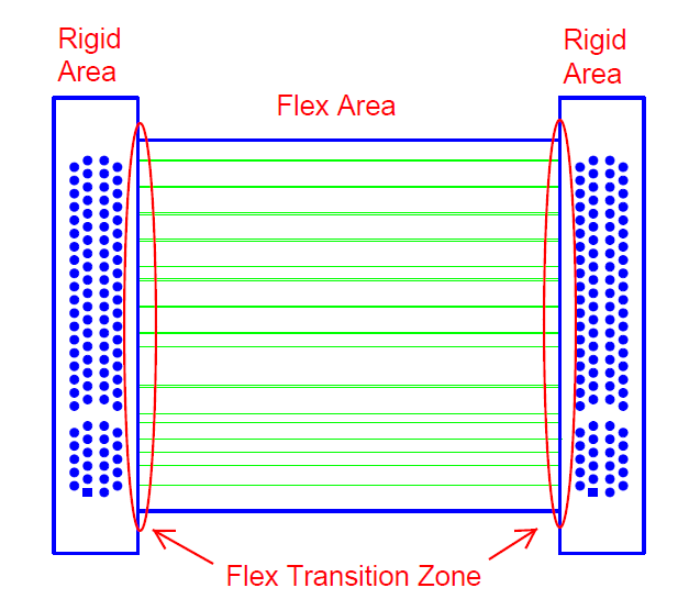
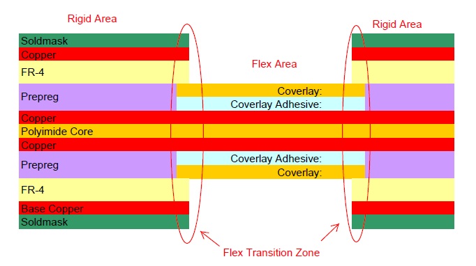
The flex transition zone is the region along the rigid circuit board outline where the layer structure changes from rigid construction to flex-only construction. This zone exists because flex coverlays must extend slightly into rigid areas.
This extension:
- Allows the flex coverlays to be captured during rigid-layer lamination
- Ensures a gapless transition between rigid and flex sections
- Complies with IPC 2223C requirements for flexible printed boards
Flex coverlays extend only a short distance into rigid areas and do not continue throughout the rigid sections.

Top View Example of the Flex to Rigid Transition Zones

Side View Example of the Flex to Rigid Transition Zones
Plated Through Hole (PTH) Spacing to Flex Transition Zones
Minimum Spacing Requirement
- Minimum clearance: 0.050 inches from the flex transition zone
Why This Spacing Matters
Maintaining this spacing prevents plated through holes from being drilled through flex coverlays as they are captured by rigid-layer lamination.
Key considerations include:
- Flex coverlays are laminated using flexible acrylic- or epoxy-based adhesives
- These adhesives have a high coefficient of thermal expansion
- PTHs drilled through coverlays experience significant Z-axis expansion and contraction during assembly reflow and product operation
Drilling through coverlays has been identified as a primary root cause of cracked hole plating, which can lead to immediate failure or latent reliability issues. This requirement is defined in IPC 2223C, Section 5.2.2.3.
External Layer Copper Feature Spacing
Minimum Spacing Requirement
- Minimum clearance: 0.025 inches from the flex transition zone
Manufacturing Rationale
This spacing ensures reliable external layer imaging during fabrication. Before final lamination, flex areas are removed from rigid production panels. This removal creates internal edges at the height difference between rigid and flex areas.
Adequate clearance:
- Allows external image transfer films to bridge these internal edges
- Ensures proper film adhesion
- Supports a consistent and reliable imaging process
A minimum spacing of 0.025 inches provides sufficient margin to accommodate these manufacturing conditions.
Via Usage in Flex Circuit Areas
Vias in flex circuit areas are not recommended and should be avoided whenever design flexibility allows.
Primary concerns include:
- Increased cost due to additional drilling and plating steps
- Requirement for blind via manufacturing processes
- Creation of mechanical stress concentrators in flex layers
These stress points may lead to breakage if the flex circuit is bent near the vias.
If Flex Area Vias Are Required
When vias in flex areas cannot be avoided:
- Locate vias away from specific bend locations
- Have the fabricator review the design to assess potential risk factors
Supplier review is important to determine whether via placement poses reliability concerns during forming or operation.
Trace Routing for Mechanical Reliability
Trace layout within flex areas plays a critical role in long-term performance once the circuit is bent into position.
Recommended practices include:
- Keep traces straight and parallel whenever possible
- Use curved corners when direction changes are required
- Minimize direction changes to reduce mechanical stress
Curved routing helps eliminate stress concentrators that may otherwise cause trace breakage during bending.
Staggering Traces Between Layers
When multiple flex layers are present, stagger traces on adjacent layers instead of stacking them vertically.
This approach reduces the “I-beam effect,” which occurs when traces are positioned directly above one another from layer to layer. Staggering improves flexibility and overall reliability in flex sections.
Key Layout Specifications:
- PTH to Flex Transition Zone Clearance = 0.050 inches
- External Copper to Flex Transition Clearance = 0.050 inches
Summary
Rigid-flex PCB designs require disciplined Gerber layout practices to balance manufacturability, mechanical flexibility, and long-term reliability. Minimum spacing rules, controlled flex-to-rigid transitions, careful via placement, and optimized trace routing all play a critical role. Addressing these requirements during layout helps prevent costly rework and reliability failures in production.
If you are developing a rigid-flex design, review these layout requirements early and involve your fabrication partner to validate risk-sensitive areas before release.
Frequently Asked Questions
Quick Links:
- How does IPC 2223C apply to rigid-flex PCB layouts?
- What is the Flex Transition Zone?
- Why must plated through holes be kept away from flex transition zones?
- Why are vias discouraged in flex circuit areas?
How does IPC 2223C apply to rigid-flex PCB layouts?
IPC 2223C defines design requirements for flexible printed boards, including how flex coverlays interact with rigid areas. The standard specifies coverlay extension and spacing rules to prevent reliability issues at flex-to-rigid interfaces.
What is the Flex Transition Zone?
The flex transition zone is the area along the rigid outline where construction changes from rigid layers to flex-only layers. It exists to allow flex coverlays to be captured during rigid lamination and ensure a continuous, gapless transition.
Why must plated through holes be kept away from flex transition zones?
Drilling PTHs through coverlays exposes high-CTE adhesives to thermal cycling stress. This stress can crack hole plating during assembly or product operation, leading to immediate or latent failures.
Why are vias discouraged in flex circuit areas?
Vias increase manufacturing cost and can act as mechanical stress concentrators. When flex sections are bent, vias near bend locations may cause layer or copper breakage.
Key Takeaways
- Flex to Rigid Transition Zones: Coverlays must extend slightly into rigid areas to ensure a gapless transition, meeting IPC 2223C standards. This prevents reliability issues at the rigid-to-flex interface.
- Plated Through Hole (PTH) Spacing: Maintain at least 0.050” clearance from the flex transition zone to avoid PTHs being drilled through coverlays, reducing risk of cracked plating and long-term failures.
- External Copper Feature Spacing: Ensure a 0.025” minimum clearance between external copper features and flex transition zones to allow reliable imaging and lamination.
- Flex Area Vias: Avoid vias in flex regions whenever possible, as they increase cost and create stress concentrators. If necessary, keep them away from bend locations and review the design with your fabricator.
- Flex Trace Layout: Use straight, parallel traces with curved corners where direction changes are needed. Stagger traces on adjacent layers to minimize the “I-beam effect” and improve flexibility and reliability.


