


Flex circuits have many unique capabilities to solve design challenges. One of these is a lap joint capability that allows a flexible circuit board to be directly attached to another circuit or component eliminating the need for any type of connector.
In this blog post, we will review the type of applications that may benefit from a lap joint flex circuit design, the design elements of this configuration, and the assembly methods used.
Definition of a Lap Joint
A lap joint, in this discussion, is defined as a direct attachment of a flex circuit to either a rigid PCB, another flex circuit, or an electronic device, i.e.: a display unit with integrated circuitry, bare die, or flip chip.

The connection is achieved using either soldering, conductive epoxy adhesives, or an anisotropic adhesive. Which method is used will depend upon the materials of the unit that the flex circuit is being attached to and the size/pitch of the contact pads. Attachment to a rigid PCB will most likely be a soldered connection as there are no temperature restrictions with either circuit and the connection pad sizes are usually large enough to allow for the soldering process. If the other circuit cannot withstand soldering temperatures, such as a polyester flex circuit, and the connection pads are still large enough then a conductive epoxy adhesive can be used as it doesn’t need any significant heat to process. If the flex is being attached to a component, such as a display unit, then an anisotropic adhesive film will be needed due to the display not being able to withstand solder reflow temps and the size and high pitch of the contact pads are usually well below what is capable with soldering or conductive epoxy adhesives.
An anisotropic adhesive is like a PSA (double-sided adhesive tape) but has the unique property of being conductive in the Z-Axis (thickness) only. The vertical connection paths within the adhesive are very dense which allows for very small and fine pitch contacts without creating electrical shorts between adjacent contacts. A 0.005” contact finger on 0.010” centers is a common design configuration.
Applications That Benefit From Lap Joints
Lap joint applications fall primarily into two groups. The first is driven by a lack of vertical space that does not allow for the height of any type of connector. Accounting for the thickness of the flex and the solder or adhesive joint a lap joint will be 0.010” or less in total height. While there are very low-profile stacking and ZIF connectors a lap joint will be considerably thinner.
The second application is driven by the size and pitch of the contact pads on the mating component and will require the use of an anisotropic adhesive and its high-density interconnect capabilities. Most of these types of allocation are connections to either display units, bare dies, or flip chips but can also be used in flex to rigid PCB or flex to flex interconnects.
Flex Circuit Design
The design of the flex circuit will depend upon the application and how the lap joint will be assembled. For low quantity or prototype applications using a manual soldered connection method, the flex circuit is designed as a min. 2-layer design even if the circuit pattern only requires one layer. This allows the inclusion of a matching set of pads on the opposite side of the lap joint pads. The stacked pads are then interconnected with several vias. These vias serve two purposes: thermal conduits to transfer soldering heat from the top side of the flex circuit to the underlying pads where the solder joint occurs and as an inspection mechanism. The solder during reflow will flow up into the vias and allow for visual inspection/confirmation of what is otherwise a hidden solder joint. The soldering method(s) will be discussed in more detail later in this blog. The pad size and pitch used also need to be large enough to allow for the soldering operation.
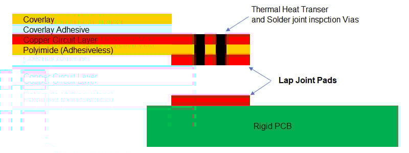
Example of a 2-layer lap joint flex stack-up.
For an automated soldering process, the flex can be created as a 1-layer design as the more controlled and reliable automated hot bar process doesn’t need the assistance of the 2 layers with via configuration.
For designs using a conductive adhesive, the flex circuit can be created with as little as 1 layer, depending upon what the schematic requires, as there is no need for heat transfer or inspection of the hidden adhesive joint.
Designs using an anisotropic adhesive are typically always 1-layer circuits and again do not have any heat transfer or additional inspection requirements.
Some potential additional design elements:
- Added tooling holes, to accept temporary tooling pins to ensure and maintain alignment between the flex and the rigid PCB during soldering.
- Local PSA (pressure sensitive adhesive) to act as a mechanical strain relief or to facilitate holding the parts in position during soldering.
Assembly Methods
As with the flex circuit design, the method used for the assembly process will depend upon the application and the expected volume of parts to be assembled. A soldered attachment can be performed either manually or using a semi-automated hot bar soldering system. With either method, the first step is to apply and reflow solder on the rigid PCB lap joint pads as part of the assembly process of the rigid PCBs components.
Prior to the lap joint soldering, a no-clean flux is applied to the pre-soldered pads. The flex circuit is positioned in place. Sufficient heat is then applied to reflow the previously applied solder on the rigid PCB again. After the solder reflows, a small amount of pressure is maintained for a short duration to ensure intimate contact between the soldered pads and to allow the solder to solidify.
A manual process will use a soldering iron as the heat source and each pad will be soldered individually. This is generally only suitable for prototypes and very small volume production quantities. For higher volumes, a hot bar soldering system is used. As the name implies these systems consist of a high temp hot bar that then compresses down on all the lap joint pads simultaneously and solders all in one step. These systems require tooling systems to position and hold the parts in place during the soldering operation. The required tooling can be costly depending on how the hot bar system is configured. Some systems have rotating beds which allow for a load/unload position in addition to a soldering position.
For flex circuit designs using an anisotropic adhesive, per the material specifications, a version of the hot bar system must be used. Heat and pressure with a specific time duration are required to correctly bond the adhesive.
Summary
Direct or lap joint soldering can be a very useful solution for a flexible circuit board design with either very restricted vertical spacing or high-density interconnects with other devices. Please feel free to contact Epec to discuss your requirements and to evaluate the effectiveness of a lap joint-based solution in your design.
Key Takeaways
- Lap Joints Eliminate Connectors: Lap joints enable direct attachment of flex circuits to rigid PCBs, other flex circuits, or devices like displays, reducing overall assembly height to 0.010" or less and saving space compared to low-profile connectors.
- Multiple Attachment Methods: Connections can be made using soldering, conductive epoxy adhesives, or anisotropic conductive films (ACF), with the choice depending on pad size, pitch, and the temperature tolerance of the mating component.
- Anisotropic Adhesives for Fine-Pitch Applications: For high-density, fine-pitch connections (e.g., 0.005” contacts on 0.010” centers), anisotropic adhesives provide Z-axis conductivity without creating shorts between adjacent pads, making them ideal for displays, flip chips, and bare dies.
- Design Features for Reliability: Flex circuits may include dual-layer lap joints with vias for improved solder heat transfer and joint inspection, added tooling holes for alignment during assembly, and localized PSA for strain relief and positioning.
- Assembly Options for Prototypes vs. Volume: Prototypes often use manual soldering with an iron, while high-volume production employs semi-automated hot bar soldering or specialized equipment for ACF bonding to ensure consistent, reliable joints.


