


At the conclusion of our webinar, Electrical vs Mechanical Requirements in Flex & Rigid-Flex PCB Designs, we had several questions submitted to our presenter, Paul Tome, Product Manager Flex and Rigid-Flex, at Epec. We have compiled these questions into a readable format on our blog.
Q&A From Our Live Flexible PCB Webinar
Quick Links:
- Can thinner copper combined with a thinner flex core be used for an impedance-controlled design to reduce the flex thickness and improve the bend capability?
- What prevents EMI shielding film from being used as a controlled impedance reference plane?
- Can older Silver Ink shielded designs be converted to EMI shielding film?
- What copper thicknesses are available for higher-current applications?
- Related to FPC controlled impedance, how significant is the influence of FR4 (or other materials) stiffener to the impedance?
- In an air gap construction, do the min. via hole sizes and pad sizes remain the same?
Watch the Recording Below:

Question: Can thinner copper combined with a thinner flex core be used for an impedance-controlled design to reduce the flex thickness and improve the bend capability?
Answer: The challenge there is that there aren't any material thicknesses available that allow you to create a manufacturable construction. So, for example, 100 on differential, half-ounce copper, two-layer strip line surface microstrip configuration utilizes a 2-mil core. The next smaller, thinner core thickness is 1 mil. There's nothing between one and two, unless you get into special order materials, obviously. But your standard goes from 2 mil down to 1 mil. Now, if you would try to use that 1 mil configuration or 1 mil thick core, you would have to use one-third ounce copper or even one-quarter ounce copper, and your line width would become less than two. That puts you now at a very, very high level of technology. Your supply chain becomes minimized. You've added a tremendous amount of expense to the design, so in most cases, not a practical solution.
Question: What prevents EMI shielding film from being used as a controlled impedance reference plane?
Answer: The material was not designed for this purpose (increased tolerances +/-20% maybe) and the increased coverlay thickness to achieve the required dielectric spacing exceeds EMI shielding adhesive capability.
Question: Can older Silver Ink shielded designs be converted to EMI shielding film?
Answer: Yes. We've done many, many designs that started off or existed as EMI or silver ink shield designs and converted them over to EMI shielding film configurations, which provided the benefit to the customer of improved mechanical bend reliability because of the thinner construction and also reduced cost.
Question: What copper thicknesses are available for higher-current applications?
Answer: Up to 2 OZ is standard. Greater than 2 OZ may require a special order or made by attaching sheet copper to a polyimide core with an adhesive layer. An additional 1 OZ, for a total of 3 OZ, can be achieved by surface plating the circuits.
Question: Related to FPC controlled impedance, how significant is the influence of FR4 (or other materials) stiffener to the impedance?
Answer: FR4 stiffeners, polyimide stiffeners, and PSAs do not have any measurable impact on the impedance values. Only if you use a stainless or aluminum stiffener would we need to review further. The coverlays do have any impact as they reside immediately on the signal layer. We’ve yet to see a modeling software that will allow coverlays to be included. We adjust for coverlays using historical data gathered from test results from finished parts.
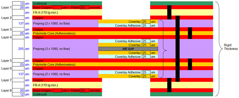
Question: In an air gap construction, do the min. via hole sizes and pad sizes remain the same?
Answer: In an air gap construction the min. via hole sizes and pad sizes remain the same. The available via structures are: blind vias from the external layer to the “next” layer (rigid layers only); buried via from the 2nd layer to the 2nd last layer (rigid layers only); and buried vias in each flex pair. In addition to a standard thru via, the following is an example of all the blind & buried via options in an 8-layer air gap construction:
Key Takeaways
- Impedance-controlled flex designs face material limits: Using thinner copper with a thinner flex core may improve bendability, but manufacturable constructions are constrained. Moving below standard 2-mil cores requires ultra-thin copper, which drives up cost and complexity while limiting supply chain options.
- EMI shielding film cannot replace a reference plane: Shielding films are not engineered for controlled impedance. Their tolerances and adhesive thickness exceed what’s needed for stable dielectric spacing, making them unsuitable as reference planes.
- Converting silver ink shields is practical: Many legacy silver ink shield designs can be upgraded to EMI shielding films. This conversion reduces cost while improving mechanical bend reliability due to thinner construction.
- Copper options vary for high-current needs: Standard flex designs support up to 2 oz copper. Beyond this, special order materials or adhesive-bonded sheet copper may be used, and surface plating can add an additional ounce to achieve 3 oz.
- Stiffeners and vias in flex require specific consideration: FR4, polyimide, and PSA stiffeners have negligible impact on impedance, while metals like aluminum or stainless steel may require review. In air gap constructions, via hole and pad size limits remain unchanged, supporting blind, buried, and standard through-vias depending on the layer configuration.


