


I have spoken in the past about my long career in printed circuit board (PCB) manufacturing (1982) and how, at the beginning of my career, we still had home phones tied to the wall by cord. If we were lucky enough, the spiral stretch cord was very long.
As consumer desire pushed forward, technology changed quickly, at least it seems like it. I remember it like yesterday (1990) watching Pretty Woman in the theater. It’s a good movie, but there is this scene on Rodeo Drive with a person on the phone in their car. It was a big phone, but nonetheless a mobile phone with someone in a car chatting; that was so cool.
Fast forward a few years, and we all started to carry cell phones, yet much smaller versions. The desire to be connected and do more was upon us and in full swing. Much of the success of this product was due to the PCB product advancements.
HDI Printed Circuit Boards
The high-density interconnect (HDI) PCBs are the critical component of all modern electronics. When it comes to miniaturization, performance, and signal integrity, it all starts with the raw PCB. As multilayer circuit boards became more widely used, the stack-up had to evolve to allow consumer products to improve their function while decreasing the desired size.

Enter HDI PCBs. The capabilities due to the complexity are amazing. Processing microvias, buried vias, and blind vias into a sequence of lamination, and here we are surfing the Internet, texting, talking, conference calls, FaceTime, and more. So, what goes into this technology?
Understanding advanced stack-ups is key to the successful design of the product.
Here’s are some terms to keep in mind:
- Signal Integrity (SI): Controlling impedance (typically 50Ω single-ended or 100Ω differential) in reference to ground planes and the proximity to the signal layers.
- Power Integrity: Making sure to include solid power and ground planes. Use power distribution networks (PDNs) with low inductance paths.
- Understanding Via Structures, Microvias: Laser-drilled: <150 µm diameter, used for layer-to-layer connections.
- Buried Vias: Connect internal layers without surface exposure.
- Blind Vias: Connect outer layers partially through to a mid-layer.
- Stacked Vias vs. Staggered Vias: Stacked saves space but requires strict manufacturing controls.
- Via in Pad: Vias inserted in pads that are used for components yet drilled, filled, planarized cap plated, and invisible to the eye when done correctly.
Sequential lamination, or the sequence of drilling/plating and lamination, is not an easy process; it takes specialty equipment, engineering, and time. It is required for stacking microvias across multiple layers, and it enables high layer counts while managing Z-axis space.
Stack-ups and Technology
Common HDI stack-up configurations are not easily processed and can have limitations by your supplier; seek advice early on from your manufacturer before design completion. Also note that:
- 1+N+1 HDI Stack-Up has one HDI layer on top and bottom of a core; it is cost-effective, entry-level, and ideal for smartphones or other handheld items.
- 2+N+2 or 3+N+3 HDI Stack-Up is when two or three build-up layers are on both sides of a core and support stacked microvias. Using this technique improves routing density for BGAs and improves the overall footprint of dense construction.
- Any-Layer HDI (AL-HDI) is a new advanced technology not commonly used but available through some suppliers. This technology comprises of microvias between any layers with maximum flexibility and routing density. This process is used in high-end smartphones, medical devices, and aerospace applications. It is very expensive due to multiple laminations and laser drills. Yield can be an issue; therefore, an engineering review at quote is necessary for costing requirements.
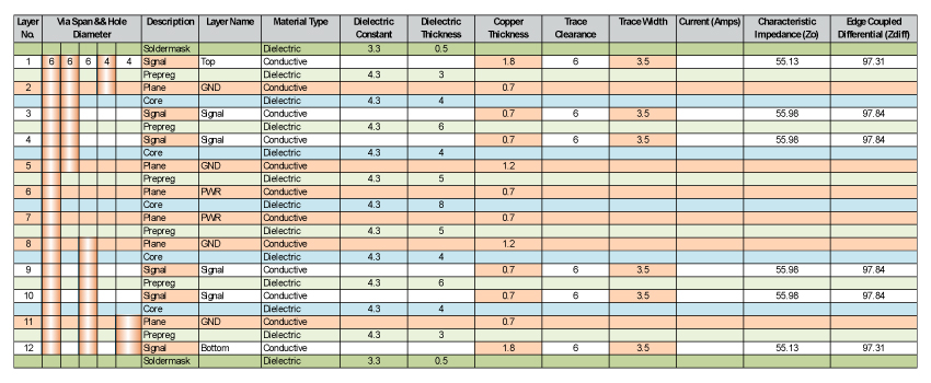
Example of a 12-layer stack-up for an advanced HDI PCB.
Stack-up design tools and techniques have their own set of parameters to follow and criteria that will push the design to additional layers or smart technology. With simulation Tools, designers will use tools like Ansys SIwave, Cadence Allegro, or HyperLynx for SI/PI and impedance control designs.
Some design rules to follow are:
- Keep high-speed signal layers adjacent to planes.
- Minimize stub lengths on via transitions.
- The use of backdrilling has become more popular, an older technology to remove plating partially from the hole, and in most cases, is used if through-hole stubs are unavoidable.
Summary
Designs are typically 100% complete when brought to Epec for production. This higher technology usually requires a manufacturing review prior to a quote to determine if it is within our current manufacturing capabilities. HDI PCBs cannot be produced in a standard manufacturing setting due to processing requirements. Coming up with a plan or traveler for producing an order is typical.
At Epec, utilizing our always-free DFM process will allow real-time review by engineering to resolve most technical issues in tandem with a manufacturing review at quote. Design for manufacturing reviews allow for correction, modification, and clarification upfront, avoiding delays to production and costly prototyping failures.
Key Takeaways
- HDI PCBs enable miniaturization and performance: Advanced stack-ups with microvias, blind vias, and buried vias allow modern electronics to be smaller, faster, and more reliable while supporting high signal integrity.
- Sequential lamination is critical for complex builds: Stacked microvias across multiple layers require precise drilling, plating, and lamination processes, making HDI boards highly specialized to manufacture.
- Different HDI stack-up options serve different applications: 1+N+1 is cost-effective for handheld devices, 2+N+2 or 3+N+3 support dense BGA routing, and Any-Layer HDI offers maximum flexibility for aerospace and medical but at higher costs and lower yields.
- Design rules directly impact manufacturability: Key practices include keeping high-speed signal layers near planes, minimizing via stub lengths, and applying methods like backdrilling to improve signal performance.
- DFM reviews are essential before production: Because of their complexity, HDI stack-ups must go through engineering and manufacturing review to confirm feasibility, avoid costly errors, and ensure reliable production.


