


Printed circuit boards (PCBs) are the heart of electronic products as they provide the conductive pathway for all the electronic components to connect and function together. As electronics become more advanced and complex, PCBs are having multiple layers sandwiched together to establish all the necessary connections.
To route electrical connections between the layers, holes are drilled entirely through the PCB, thus connecting all the layers together when the holes are plated with copper. These are called plated through-holes or vias. Depending on the diameter, the hole may be considered a microvia.

What is a Microvia?
According to the Institute of Printed Circuit Boards (IPC), a microvia is any hole drilled into a PCB that has 1:1 aspect ratio but doesn't exceed a 0.010-inch depth. Previously, the IPC considered microvias based on their size if it was equal to 0.006 inches or smaller. However, changing technology now allows lasers to drill such small holes frequently.
The IPC decided on the new microvia definition of the 1:1 aspect ratio and 0.010-inch depth threshold to prevent constantly changing their definitions. Microvias, also referred to as uVias, may be used to connect layers within the PCB. Yet they usually do not connect more than two layers in succession.
Different Types of Microvias
There are many types of microvias that PCB designers can drill. Each type of microvia has the same size aspect ratio. The main difference between them is their placement.
- Blind Microvias - drilled to allow for connections from the surface to another inner layer. These holes do not go completely through the PCB like a through-hole and are from one side.
- Buried Microvias - holes in an inner layer of the PCB that do not reach any external surface of the circuit board.
- Stacked Microvias - several blind and or buried microvia stacked on top of each other allowing for the inner layers to be connected.
- Staggered Microvias - are multiple buried microvia connecting layers. These microvia are not stacked on top of each other. Instead, they are placed offset from one another.
- Via-In-Pad Microvias - involve placing the microvia holes directly on the copper solder pad of the component. This technique allows for PCBs to be miniaturized.
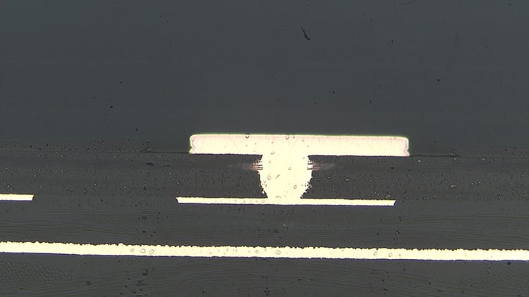
Example of a copper plated shut mechanical depth drilled microvia.
Advantages of Microvias for PCB Designers
PCB designers may find many benefits in using microvias for circuit boards designs. Microvias offer thermo-mechanical reliability to the functions and performance of the board. With circuit boards becoming smaller and lighter to fit into mobile devices, the ability to create via-in-pad microvias allows for miniaturization of the boards. Microvias save space on the circuit board due to their size that is smaller than a normal via or plated through hole. By saving space, you do not have to have larger boards to fit all of the necessary components that will be connected.
PCB designers can also minimize their risks of defects with microvias, as lasers are used to drill the holes. There are less fabrication issues to experience as trace lengths are shorter. If creating HDI circuit boards, microvias create significant impacts on signal integrity. When creating larger vias, higher amounts of radiation is created for the high-speed circuits. When placing in microvias, RF capabilities become enhanced along with EMC characteristics. Microvias offer greater reliability than other types of vias and through holes.
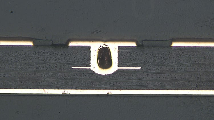
Example of unfilled mechanical depth drilled microvia.
When Designing Microvias on PCBs
There are several aspects about drilling microvias for PCBs. When designing a circuit board, keep in mind that when you are looking for a hole that can be reliably plated, the microvia should not go above the 1:1 aspect ratio. While it is true that it can be drilled at a larger ratio, it simply will not be reliable as it will likely result in plating defects. In addition, our PCB designers will not go below a 4-mil diameter regardless of the aspect ratio. When first drilling into the copper surface with a laser drill, the PCB design should not have copper that exceeds 1/2 oz. As thicker copper is added, it makes the laser work harder to make the hole and ablate down to the next adjacent layer.
When placing it in multiple layers, each layer that receives a via will need to have an additional lamination step. Holes that will not be used can be non-conductively filled or plated shut if desired. Since microvias are so small, they may not need to be filled. Copper is used for the plating, as a specialized bath and chemistry created for the process is produced. Using this process, the fabricator gains more flexibility in the design process.
If a layer is skipped, such as blind microvias going from a first layer to a third layer, there will need to be clearances along the second pass through layer. However, if the second layer needs to become connected to the third layer, then microvias that are stacked or staggered can be used. However, staggered vias are easier to fabricate and provide more reliability.
Summary
Microvias offer PCB designers flexibility with the fabrication process as customers obtain reliability when connecting multiple layers. When selecting materials for the printed circuit boards, there are some materials that are more suitable for the microvia drilling process.
Speaking with the PCB fabricator prior to selecting the material set allows you to understand the available options. Epec engineers have extensive experience helping people select the materials that are suitable for the application while being able to connect your electrical components. Also, you may be able to cut down on material costs using different microvia drilling processes. By using vias, you may be able to order smaller boards while saving space. You may encounter significant cost savings while receiving PCBs with minimal manufacturing defects and risks.
Key Takeaways
- Microvias are defined by size and aspect ratio: Microvias are PCB holes with a 1:1 aspect ratio and a depth of no more than 0.010 inches, typically used to connect one or two adjacent layers. This definition helps standardize designs despite evolving laser drilling capabilities.
- There are multiple types of microvias: Microvias include blind, buried, stacked, staggered, and via-in-pad variations. Each type serves a specific layout or space-saving function, especially useful in high-density interconnect (HDI) designs.
- Microvias enable smaller, high-performance PCBs: Because of their small size and laser precision, microvias reduce trace lengths, enhance signal integrity, and allow for more compact, lightweight circuit board designs—ideal for mobile and high-speed electronics.
- Design considerations impact reliability: To ensure microvias can be plated reliably, designers should maintain a 1:1 aspect ratio and avoid laser drilling through thick copper. Staggered microvias are generally preferred over stacked ones for better manufacturability and reliability.
- Early collaboration with fabricators is critical: Speaking with your PCB fabricator during the material selection and design phase helps prevent defects, manage costs, and optimize microvia drilling. The right material set and drilling process can lead to improved performance and cost savings.


