Within the printed circuit board industry the term "tenting" originally indicated that the mask would fully enclose the via at one end by forming a skin or tent over the opening. While dry film solder mask is more expensive, it is capable of forming a reliable tent, while liquid photoimageable solder mask (LPI) generally will not.
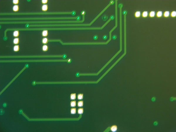
With LPI solder mask, circuit board via tenting has come to mean that the mask will cover the pad and enter the hole, but will not close the hole completely. Via filling is used where the via must be closed. There are two types of material that can be used to fill a via, which can be either conductive or non-conductive. As seen in the image below; the back light shows that the vias are not plugged, but the annular ring is covered with mask. The tent over the hole can be broken, as long as the annular ring is covered.

Tenting Vias of a Printed Circuit Board Under a Microscope
LPI tenting is used primarily to reduce the number of exposed conductive pads which are present on the PCB surface. The goal is to reduce the likelihood of shorts caused by solder bridging during the assembly process. It also helps to reduce paste migration away from SMT pads when vias are placed on the ends of SMT pads, or on BGA dog-bones.
Tenting vias is useful wherever SMT pads are placed in close proximity to vias. It is particularly useful within BGA areas, where reworking shorts underneath the component is difficult and time-consuming.
Feel free to visit our printed circuit board and PCB via process page for further information, or download our ebook on PCB design below!


