In modern electronic systems, the need for high-speed data transmission has never been greater. With faster clock speeds, smaller geometries, and increasing complexity in printed circuit board (PCB) layouts, ensuring signal integrity has become a top priority for designers. Consulting your PCB manufacturer should be at the top of your list.
Signal integrity (SI) refers to the quality and reliability of the electrical signals as they travel through a PCB. Poor signal integrity can lead to data corruption, timing errors, and even system failure.
This blog post explores the fundamentals of signal integrity, its significance in high-speed PCB design, and best practices for ensuring robust and reliable designs. Even more importantly, having a close relationship with your suppliers is critical to your end project functionality.
Understanding Signal Integrity
Signal integrity involves analyzing and controlling how electrical signals behave over transmission lines in a PCB. In an ideal world, a digital signal would resemble a perfect square wave. However, signals experience degradation due to various factors such as reflection, crosstalk, electromagnetic interference (EMI), and power integrity issues. These problems become more pronounced at higher frequencies and faster edge rates.

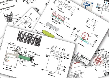
The signal travel is extended by the bump and weaving portion of the traces.
The key elements that affect signal integrity include:
- Impedance Control: Maintaining consistent characteristic impedance throughout a signal path is crucial to avoid reflections.
- Signal Reflections: Occur when there is a mismatch in impedance, causing signals to bounce back toward the source.
- Crosstalk: Undesirable coupling between adjacent traces, which can induce noise and cause false switching.
- Ground Bounce and Simultaneous Switching Noise (SSN): Voltage fluctuations in the ground plane can cause logic level errors.
- Timing Jitter and Skew: Variability in signal timing can lead to incorrect data interpretation.
Why Signal Integrity Matters in High-Speed Design
As data rates exceed hundreds of megahertz and into the gigahertz range, the PCB traces start to behave like transmission lines. At these speeds, traditional low-frequency design approaches are no longer sufficient.
Ignoring SI issues can result in:
- Unpredictable circuit behavior
- Bit errors in data transmission
- EMI problems and regulatory non-compliance
- Increased design iterations and time-to-market delays
That is why incorporating signal integrity considerations early in the design phase is essential.
Best Practices for Ensuring Signal Integrity
High-speed circuit board designs demand more than just connecting traces from point A to point B. To ensure reliable performance, engineers need to plan carefully and adopt techniques that protect signal quality throughout the PCB.
You’ll want to consider these best practices:
- Plan Layer Stack-up Carefully - A well-thought-out layer stack-up is the foundation of signal integrity. Use a symmetric stack-up with alternating signal and plane layers to minimize loop area and EMI. Place signal layers adjacent to power or ground planes to provide return paths and controlled impedance.
- Use Controlled Impedance Traces for high-speed signals, calculate and control the impedance of traces using appropriate PCB materials, trace width, spacing, and height above the reference plane. Use tools or impedance calculators to ensure 50-ohm or 100-ohm differential impedance as required.
- Minimize Trace Lengths and Use Matched Lengths - Longer traces can introduce delays and increase the chance of reflections. Keep the traces as short as possible and match lengths in differential pairs and parallel buses to reduce skew.
- Ensure Proper Termination - Terminating high-speed lines with resistors helps to match impedance and absorb reflections. Common termination methods include series termination, parallel termination, and Thevenin termination.
- Avoid Via Stubs and Reduce Discontinuities - Vias introduce impedance discontinuities that can reflect signals and distort waveforms. Use back-drilling or blind/buried vias to reduce stub lengths. Ensure smooth transitions between layers.
- Optimize Signal Routing - Route high-speed signals on inner layers between ground planes to shield them from EMI. Use microstrip or stripline configurations to control impedance. Avoid 90-degree bends; use 45-degree or curved traces instead.
- Isolate Noisy and Sensitive Signals - Keep digital, analog, and power signals separate. Route high-speed or noisy signals away from sensitive analog traces. Use guard traces or ground planes to isolate critical signals.
- Manage Power Integrity - A noisy power supply can degrade signal integrity. Use a solid ground plane, sufficient decoupling capacitors, and low-inductance power delivery networks (PDNs). Proper power plane design helps minimize voltage drops and ground bounce.
- Utilize Differential Signaling Where Appropriate - Differential pairs (e.g., USB, HDMI, Ethernet) are less susceptible to noise and have better EMI performance. Route them together with consistent spacing and length to maintain impedance and timing.
- Simulate and Analyze Early Use Signal Integrity Simulation Tools (e.g., HyperLynx, SIwave, Ansys, Altium) to model signal behavior before fabrication. Simulate for reflections, crosstalk, eye diagrams, and jitter to identify and mitigate issues early.
Tools and Technologies Supporting Signal Integrity
Modern PCB design software offers various tools to assist with signal integrity:
- Impedance Calculators: For determining trace dimensions.
- Signal Integrity Analyzers: Simulate signal paths and identify SI problems.
- 3D Field Solvers: Provide accurate modeling of complex geometries.
- Eye Diagram Analysis: Visual representation of signal quality at the receiver.
Additionally, hardware validation using oscilloscopes, time domain reflectometers (TDRs), and vector network analyzers (VNAs) can help verify SI in prototypes.
Common Pitfalls to Avoid
Even experienced designers can fall into traps that compromise SI:
- Ignoring Return Paths: Every signal needs a clear return path. Poor return path design leads to EMI and signal degradation.
- Underestimating Crosstalk: Failing to maintain adequate spacing between high-speed traces can introduce significant noise.
- Overlooking Power Integrity: A stable power supply is essential. Noise on the power rail can be coupled into signal lines.
- Neglecting Manufacturing Constraints: Designs with overly tight tolerances may be difficult or expensive to fabricate accurately.
Summary
Signal integrity is a critical aspect of high-speed PCB design that cannot be overlooked. With rising data rates and increased circuit complexity, designers must adopt a proactive approach to identify and mitigate SI issues. By understanding the physics behind signal degradation and following best practices in layout, routing, and analysis, engineers can ensure robust and reliable designs.
From meticulous layer stack planning to thorough pre-layout and post-layout simulations, every step counts. No one knows better than your PCB manufacturer about what can and cannot be manufactured. At Epec, we always provide free DFM services as well as consultations with engineers to improve your design and stack-up before production.
Ultimately, strong signal integrity translates into better system performance, fewer design iterations, and faster time to market. As technology continues to advance, mastering signal integrity will remain a cornerstone of successful electronic product development.
Key Takeaways
- Signal integrity is mission critical: Poor SI leads to data corruption, EMI issues, and system failures, making it a core consideration in high-speed PCB design.
- Controlled impedance and termination are essential: Maintaining consistent impedance and using proper termination methods reduces reflections and ensures clean signal transmission.
- Thoughtful routing improves reliability: Short, matched traces, differential signaling, and routing high-speed signals between ground planes minimize noise, crosstalk, and EMI.
- Power integrity directly impacts SI: Solid ground planes, decoupling capacitors, and low-inductance power delivery networks stabilize the system and reduce ground bounce.
- Early simulation and manufacturer consultation prevent issues: Using SI tools and working closely with PCB manufacturers during design helps catch problems early, saving time and reducing costly design iterations.


