Wave soldering, the process of attaching electronic components to the printed circuit board (PCB), becomes increasingly difficult as pitch decreases. Pitch is the center-to-center spacing between the conductors on a PCB. So knowing that wave soldering becomes harder with lower pitch measurements, what is the minimum pitch distance you should maintain on circuit boards? With the appropriate controls, it is still possible to get a good result with pitches as low as 0.5mm (.0197"). Wave soldering defects can occur in pitches below 0.5mm, so we recommend this as the minimum pitch to wave solder a PCB.
During the circuit board design stage, you need to pay close attention to component orientation and placement, and consider the following best practice details:
- Use shorter lead lengths whenever possible.
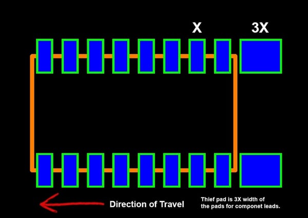
- Add solder thief pads to the PCB artwork to allow excess solder to flow away from connectors so they will be less likely to bridge.
- Control machine parameters such as temperature, immersion depth, and back flow according to manufacturer recommendations.
- Use appropriate amounts of flux.

Illustration of Solder Thief Pad in a Printed Circuit Board
Conclusion
Wave soldering printed circuit boards with surface-mount technology (SMT) pitches below 0.5mm is not recommended and could result in PCB defects. Pad size to pitch ratio becomes so small that most bare PCB manufacturers are unable to guarantee adhesion of solder mask dams between pins. When no dams are present, solder is able to flow freely across the circuit board surface, and can form bridges between adjacent pins. Not considering all factors when designing PCB for tight spaces can result in short circuits, forcing the assembler to rework the PCBA before it can be used.


