
As today’s printed circuit boards (PCBs) become smaller, they use fewer and fewer through hole components. It is increasingly difficult to justify allocating precious space for relatively large plated through component holes and their accompanying lands. Instead, it is necessary to use surface mounted components wherever possible. As surface mount technology becomes increasingly prevalent, the majority of the plated through holes on most modern PCB designs end up being vias.
The main purpose of any PCB via is to provide a conductive path for passing an electrical signal from one circuit layer to another by means of a plated hole wall. However, there are different types of vias and different options for the final appearance of the vias on the PCB surface. While all vias perform essentially the same function, each type needs to be defined accurately in your documentation so that assembly will go smoothly and your PCBA will function reliably.

Via Structures – Through, Blind, Buried:
The first type of via is the through via. This is a hole drilled all the way through from the top layer to the bottom layer. It is open at both ends to allow for plating solution to flow through and coat the hole wall to make it conductive. There is no trick to drilling through vias, provided you follow your fabricator’s rules for minimum diameter, maximum aspect ratio (board thickness divided by hole diameter), and adjacency (minimum allowable distance from the edge of one via to the nearest adjacent via).
Next come mechanically drilled blind vias. Blind vias are drilled from the top or bottom layer but stop at some point before traveling the full distance through the PCB. Mechanically drilled blind vias can be used to connect an external layer to an adjacent layer and, in certain instances, to another layer below but careful planning is required in order to guarantee a good result. Unlike a through via, a blind via is only open at one end, so plating solution cannot flow all the way through the hole. This complicates the plating process.
The most common complication is that air bubbles can become entrapped at the bottom of the holes, resulting in voided areas with no copper coverage. To counter voids, it is best to use larger holes, smaller aspect ratios, and more aggressive plating agitation which will allow the air bubbles to escape and expose the hole walls for reliable plating. Learn your fabricator’s design rules and apply them when you need to use this type of via. Proper design coupled with good process control will result in high yields.
Next are mechanically drilled buried vias. These are used to connect internal layer structures only. They are initially drilled as through holes from top to bottom of a laminated internal structure (such as from L2-L7 of an 8-layer PCB) before being plated and filled in preparation for final lamination.
Sometimes blind holes connect only internal layer pairs before being laminated over. In some high-density applications, very small external layer features such as BGA or QFP pads can be connected to the buried structures by means of laser microvias. The resulting “stacked” structure forms the equivalent of a through hole but uses less external layer real estate than would be required for a mechanically drilled through via.
Laser microvias are the smallest via type, usually around 0.003” - 0.004” in diameter. The biggest advantage of microvias is their ability to fit onto very tight land areas, most often as vias-in-pads within tight pitch SMT or BGA footprints. The pads are planarized back to their original smooth condition after plating, restoring the pad surfaces so they can be used for component soldering.
Maximum aspect ratio for laser microvias is very small -- usually around 1:1 -- so for most applications it is only practical to connect one layer to its adjacent layer through a very thin dielectric sheet. In extremely dense designs, they can be stacked one over the other in a manner like the one used for stacking a buried via, using sequential lamination.
Firstly, the vias are laser drilled, plated, and planarized to form an interconnection from the outermost layer to the next layer below it. When those steps are complete, another layer is laminated onto the outside of the stack. After lamination, the new layer undergoes another cycle of blind drilling and plating. This connects the outermost layer to the adjacent layer. This process can generally be repeated 3-4 times if necessary.
Methods for Covering or Filling Vias:
It is often desirable to perform additional treatments to the vias later in the production sequence to improve either thermal performance or assembly yield. These may include epoxy hole filling, secondary solder masking, or some combination of the two.
These additional process steps are most often intended to eliminate assembly issues such as solder shorting between a component pad to a via pad or solder migrating down through the barrel of a via which has been drilled into a component soldering land. These problems lead to costly troubleshooting and rework. Fortunately, it is possible to eliminate most issues by specifying an appropriate via treatment.
Tented vias have a non-conductive solder mask covering over the pad at both ends of the hole. Tenting was popular when dry film solder mask was in its prime, because dry film’s 0.004” thickness enabled it to tent even relatively large holes very reliably without much chance of breakdown. Today however, dry film mask is no longer used since its height causes difficulty with modern surface mount soldering. Dry film’s decline and disappearance has made this old form of tenting impractical because modern LPI solder masks are only about one tenth as thick and will not form a true tent.
Encroached vias have solder mask over most of the pad but the mask stops short of the hole by a few thousandths of an inch. This is a good compromise on medium-density PCBs between a full plug and doing nothing at all. The presence of the solder mask effectively increases the distance between the via and the nearby solderable pad, reducing the likelihood of solder bridging from the pad to the via. Since the hole is open, there is no concern about contaminant entrapment or air pocket formation in the barrel of the hole. When preparing your Gerber files, size the solder mask openings for the affected holes at hole diameter + 0.004”. Example: 0.010” via, 0.014” Gerber mask opening.
PCB Via Treatments

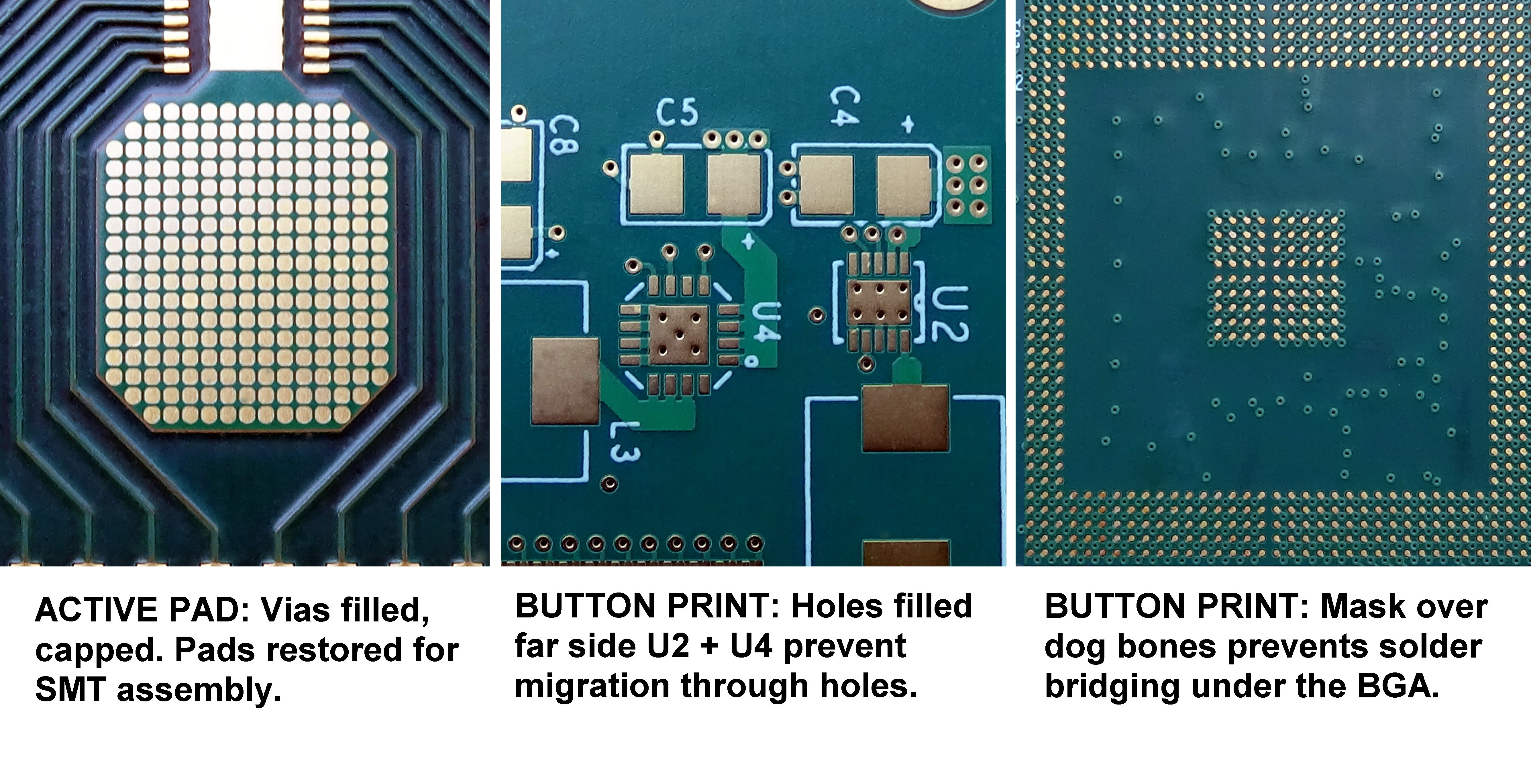
Button print and plugged via are variations on filled vias. They protect against solder flow-through (migration) so that the correct amount of solder remains on the pad during assembly. The recommended material for these processes is a non-conductive epoxy hole fill. Limit your vias to 0.020” maximum diameter to allow the epoxy to fill the hole effectively. For these types, supply your Gerber files with no solder mask openings for the vias in question.
Active pad not only plugs the hole but also plates over the plug. Commonly known as via-in-pad, cap-and-plate, or VIPPO, this is necessary if the pad through which the via was originally drilled will be used later for soldering a surface mounted component. It is also useful for cooling a hot-running component by drawing heat through the via to the opposite side of the board where it can dissipate.
In active pad processing, the plug is applied, drawn through the hole by vacuum, planarized, and over-plated. The resulting surface is often indistinguishable from other SMT pads which never underwent drilling. For this type, supply your Gerber file with no solder mask openings for the vias in question.
For more information about the via treatments described above, including pros and cons, cross-sectional views, etc., refer to our PCB plug via process page.
How to Define Via Requirements:
To avoid PCB issues, it is important that you state your via requirements for TYPE and TREATMENT clearly in your fabrication documentation so that you get what you expect. In all cases, provide a separate file for each set of vias used in the design.
For TYPE, supply your fabricator with the following information:
- Via type (through, blind, or buried)
- Via diameter (we recommend between 0.008” - 0.020”)
- Tolerance (+/-0.003” typical, although small or plugged vias may be +000/-hole diameter)
- Layer pairs to be connected by each drill file, if blind or buried.
Example: Blind vias drilled 0.008”, finished 0.008” + 0.000”/-0.008”, from TOP layer 1 to GND layer 2.
For TREATMENT, supply your fabricator with the following information:
- Process all _____ diameter vias with solder mask encroaching onto pad, but not filling hole, per Gerber file (name.)
- Plug vias (partial fill): Use button print or IPC Type 4 treatment for all _____ diameter vias using non-conductive epoxy.
- Plug via (100% fill): Use IPC Type 5 treatment for all _____ diameter vias using non-conductive epoxy.
- Fill and cap all _____ diameter vias per IPC Type VII. Fill holes with non-conductive epoxy, planarize, and plate over. Apply surface finish over pad.
Be Specific for Best Results
Any lack of clarity in your PCB fabrication notes and documentation can delay your quote, affect your bare PCB delivery, or complicate your assembly cycle. With the advent of higher density designs, clear requirements for via type and treatment take on greater importance than in the past. Remember that different contract manufacturers have different preferences and different PCB fabricators may not use all the same equipment and materials. This makes it risky for you to simply supply your Gerber solder mask files without openings for the vias expecting that one fabricator will deliver boards processed exactly like another. Instead, state all via requirements clearly and check to be sure that your data files match those requirements. A bit of time spent describing your project accurately will eliminate unpleasant surprises later.


