


Developing a successful RF printed circuit board (PCB) design requires careful consideration of various factors to ensure optimal performance and reliability. RF PCBs are essential components in wireless communication systems, radar systems, and other applications that rely on radio frequency signals.
In this blog post, we will explore some of the basic issues that engineers should consider when designing RF PCBs. From material selection to component placement and routing techniques, understanding these fundamental considerations will help engineers create high-performance RF PCB designs.
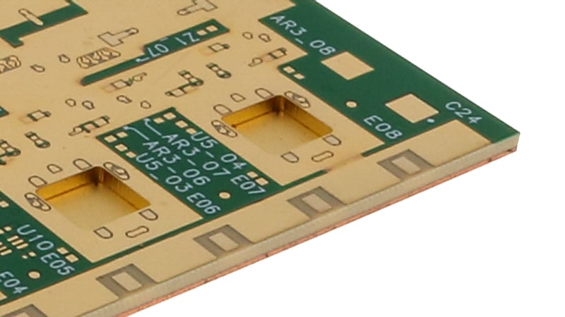
RF printed circuit board with plated cutouts.
Frequency Considerations
One of the primary factors to consider when developing an RF PCB design is the operating frequency range. The choice of frequency range influences the selection of components, material characteristics, and routing techniques. RF circuits typically operate at high frequencies, often ranging from a few megahertz to several gigahertz.
To ensure optimal performance, it is crucial to carefully select the appropriate PCB material with low dielectric loss and consistent impedance characteristics across the frequency spectrum. High-frequency laminates such as Rogers or Taconic materials are commonly used for RF PCB designs due to their excellent electrical properties.
Additionally, proper trace width and spacing become critical at higher frequencies to maintain controlled impedance. Transmission lines, such as microstrips or strip lines, should be designed with precise dimensions to match the desired characteristic impedance. Utilizing controlled impedance calculators or specialized design tools can aid in determining the optimal trace dimensions.

Component Placement and Layout
The strategic placement of components on the RF PCB plays a significant role in minimizing signal interference and optimizing performance. Careful consideration should be given to the location and orientation of high-frequency components, connectors, and antennas.
To reduce parasitic effects, it is advisable to keep sensitive RF components away from noisy digital circuits. Separating analog and digital sections can help minimize electromagnetic interference(EMI) and crosstalk. Placing RF components closer to the antenna and utilizing shorter traces can reduce transmission line losses and improve signal integrity.
Thermal management is another important aspect to consider during component placement. The heat generated by power amplifiers or other heat-producing components should be efficiently dissipated to avoid performance degradation. Adequate spacing, heat sinks, and thermal vias can assist in managing temperature levels.
Furthermore, the layout of the PCB traces should be carefully designed to minimize signal degradation and EMI. Employing proper grounding techniques, such as a dedicated ground plane and stitching vias, can help reduce noise and maintain signal integrity. Routing high-frequency traces as short as possible and using proper shielding techniques, like ground or power planes, can also enhance RF performance.
Signal Integrity and EMI
Signal integrity is crucial for reliable RF communication. Ensuring proper signal integrity involves minimizing signal loss, reflections, and distortions. This can be achieved by using impedance-matched transmission lines, controlled trace lengths, and proper termination techniques.
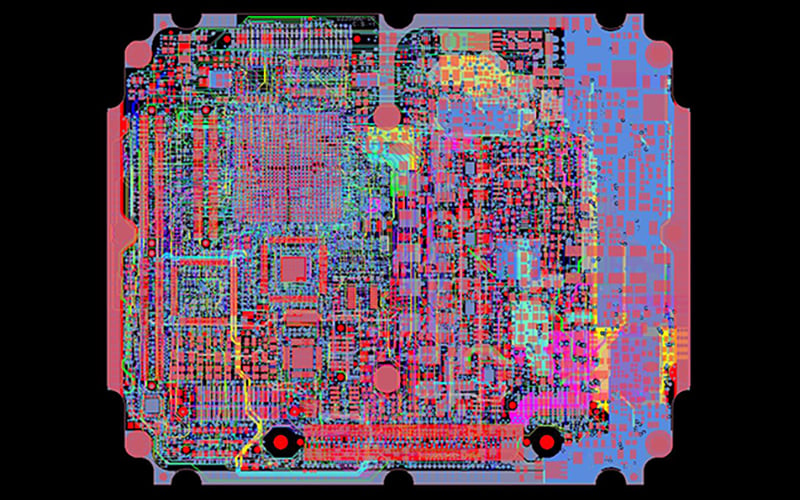
A multi-layer circuit board showing signal layers.
Controlling electromagnetic interference (EMI) is equally important in RF PCB design. RF circuits are susceptible to interference from other components, nearby devices, or external sources. Implementing good EMI shielding practices, such as using shielding cans, balanced routing, and filtering components, can mitigate unwanted noise and improve overall system performance.
Grounding plays a critical role in minimizing EMI and maintaining signal integrity. It is vital to establish a solid ground reference plane that is continuous throughout the PCB. Ground vias or stitching techniques can ensure a low-impedance ground path for high-frequency signals.
Manufacturing and Testing Considerations
When designing RF PCBs, it is crucial to consider manufacturing and testing aspects to ensure successful production and reliable performance. Collaborating closely with the PCB manufacturer is recommended to address any specific manufacturing requirements.
The manufacturing process should meet the necessary tolerances for high-frequency designs. Controlled impedance testing and verification of layer stack-up are essential steps to ensure the design meets the desired specifications.
Post-manufacturing testing is crucial to verify the performance of the RF PCB. Testing techniques such as time-domain reflectometry (TDR) can identify impedance mismatches, signal reflections, or other signal integrity issues. Testing RF circuits with appropriate instruments, such as network analyzers, spectrum analyzers, and vector signal analyzers, can validate the design's performance.
Summary
Developing an RF PCB design requires careful consideration of several fundamental issues. By considering frequency considerations, component placement, signal integrity, EMI control, and manufacturing/testing aspects, engineers can create high-performance RF PCBs.
Proper material selection, controlled impedance design, strategic component placement, and thoughtful layout techniques contribute to the overall success of an RF PCB design. With thorough planning and adherence to best practices, engineers can achieve reliable and efficient RF circuitry for a wide range of wireless communication applications.
Key Takeaways
- Material selection is critical for RF performance: Use high-frequency laminates like Rogers or Taconic to ensure low dielectric loss, consistent impedance, and stable performance across a wide frequency range.
- Controlled impedance design is essential: Precise trace widths, spacing, and the use of microstrip or stripline transmission lines help maintain signal integrity and minimize reflections in high-frequency circuits.
- Component placement directly impacts signal integrity: Keep RF components close to antennas, separate analog and digital sections, and use short trace lengths with proper grounding to reduce losses, EMI, and crosstalk.
- Strong grounding and shielding practices are required: Employ continuous ground planes, stitching vias, and shielding techniques to minimize EMI and maintain reliable RF performance.
- Manufacturing and testing must be planned early: Collaborate with your PCB manufacturer for controlled impedance tolerances and verify performance using testing methods like TDR and network analysis to ensure reliable results.


