
In front-end engineering, we must gather as much manufacturing information as possible from the printed circuit board data we receive. This includes customer service notes, customer emails, and the general spec, if available. Usually there is enough information to release a printed circuit board (PCB) package to manufacturing. However, I have found many gray areas that haunt our engineering department.
Minimum Plating in Holes
Many customer drawings have a note that states: 0.001” absolute minimum plating in the holes. When I used to run a plating line, getting 0.001” in the holes was not too difficult to achieve by simply increasing the copper plating times. This would work just fine if bath agitation, copper anodes, sulfuric acid content, brightener content, and plating amps were all working correctly. Also important is the way that you rack each board before placing them in the tanks.
Now with high volume production, automatic plating lines, 0.001” absolute minimum in the holes becomes an issue. IPC Class 2 says 0.0007” is fine. IPC Class 3 says 0.001” average, with 0.0008” minimum in the holes is fine. So, hopefully PCB designers will begin to understand, that if they believe 0.001” in the holes is needed, they will realize Class 3 (medical, aerospace, mil spec) will be just fine.

Where did this 0.001” in the holes come from?
In the past, we were told to plate one ounce of copper (an ounce of copper is 0.0014") to every standard build. We would adjust our plating time and amperage for 1-ounce plating. Lo and behold, when quality control did microsections, the plating in the holes would be 0.0008” to 0.001” or more. So, this 0.001” number generally meant, plate an ounce of copper.
To help avoid confusion, a better statement would be plate 0.001” average in the holes.
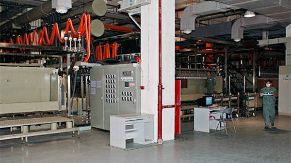
Automated PCB Plating Lines
PCB Surface Finishes
Another stumbling point are PCB surface finishes. Many military specification and aerospace drawings (often appearing to have been drawn in prehistoric times) will say follow copper with 0.0003” of tin lead 60/40. A long time ago we would rinse the circuit boards after copper plating, clean them in acid, and then throw them in the electrolytic tin lead tank for time. The longer you left them under amperage, the more tin lead you would get. Eventually the circuit board industry moved away from using lead-based finishes as much.
Along came RoHS surface finishes and HASL that use less lead. You will not get 0.0003” tin lead plated from HASL. No one uses old tin lead plating anymore.
Now, drawings will typically say 3u (millionths) gold for an ENIG surface finish. The origins of this are unknown but the general line of thinking for this was perhaps that more is better. However, IPC says 1.9u minimum is fine. ENIG is an immersion process, immersion baths plate very quickly to a surface but will not accumulate thickness very well no matter how long you leave a board in the tank. It is only a chemical process without electrolytic help. The coverings are complete but thin and still okay since solderability is the end goal anyways. You don’t need 3u, 5u, or 14u gold - 1.9u coverage will work just fine for most designs.
Immersion tin is the same. It looks great if you do not touch it, works well too, but is generally a very thin covering.
Circuit Board Copper Weights
Copper weights are another nightmare that shouldn’t be. Most PCBs need one ounce of finished copper. What this means is that internal layers will have one-ounce copper foil, usually not quite one ounce, while outer layers will start at half ounce with standard plating added. Standard plating these days on automated lines will give you a 1-ounce finish and 0.0007” in the holes. Just fine again from IPC.
The problem in front end engineering is many PCB drawings are not clear as to finished copper weight. Stack-ups may say 1-ounce copper. Alright, is it finished or starting? A lot of commercial drawings mean finished, Mil spec drawings mean starting.
The important takeaway here is to state whether it is finished or starting copper on the stack-up.
PCB Material
Most circuit board drawings say G10 or FR4 for a material callout. Typically, we use FR4. A little notation is needed on the drawings to specify which laminate material you’d like i.e. Tg130 (standard FR4), Tg170, or Tg180. It is also alright to call out the IPC4101 specific numbers which refer exactly to the required Tg temperature. Most drawings are fine.

Summary
This post is intended to help you be more specific while also simplifying your PCB drawing notes. Having accurate data, standardized PCB notes, and drawing files speeds up the front-end engineering process as well as eliminating technical questions, ensuring you receive your circuit boards faster and built correctly!


